This thread has been locked.
If you have a related question, please click the "Ask a related question" button in the top right corner. The newly created question will be automatically linked to this question.
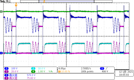
Our customer found folloing SR timing delay waveform. (delay time: about 550ns)
<Condition>
IN:DC240V-DC340V
OUT:13.5V/4A
Also they didn't found low Vin and light load condition.
CH1:Primary FET_VDS
CH2:Secondary FET_VGS
CH3:Secondary FET_VDS
CH4:Vout (AC mode)
Fsw:116kHz
Primary FET ON time:1.35us
Please let us know why these waveform is found.
They think these waveform have an impact on efficiency.
If you need any other information,please let us know it.
Regards,
Hi Kura,
The SR MOSFET turn on is determined when the SR MOSFET body diode starts conducting and the VPC pin voltage falls to near zero. from the waveform we can see the SR body diode already conducted , another turn on criteria is VPC pin voltage falls to near zero. there is a RC time constant on VPC pin which can delay the secondary voltage detection by VPC pin. R is VPC pin divider resistors and C is the VPC pin parasitic capacitance. if there is a ground plane under the divider resistors and VPC pin trace , it will worse the turn on delay.
Solution is try to reduce parasitic capacitance(remove ground plane if have and place Rvpc2/Rvpc1 as close as controller to short VPC routing trace) and decrease Rvpc2 resistance then re-calculate Rvpc1.
Thanks.