This thread has been locked.

If you have a related question, please click the "Ask a related question" button in the top right corner. The newly created question will be automatically linked to this question.

LM5175: Why does this regulator oscillate (ramp) on the output?

Part Number: LM5175

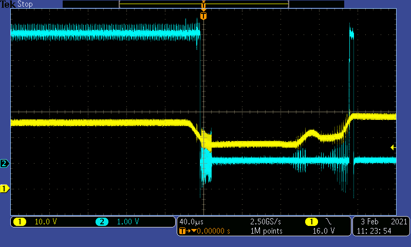
I need to take an input voltage of 14V to 24V and convert it to an output of 24V at up to 8A using the LM5175.  I used an (almost) identical layout as the TI demo board (a 6-layer design).  When the board is powered up, depending on the input voltage, I either get proper operation (with a clean, solid 24V output) or the output overshoots by 5 - 10V and ramps down to 24V whereupon it again overshoots and ramps back down.  The period of the ramp ranges from about half a second to several seconds.

Here is the schematic:

Output Reg.pdf

Note that the problem occurs even when the adjustable output feature is disabled.  That is, I have removed R195, and set R194 to 16.5K.

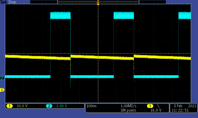
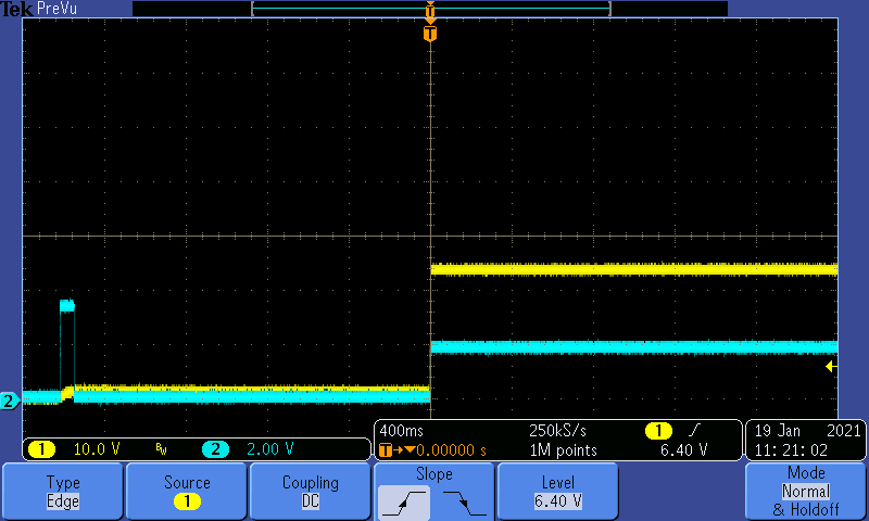
WORKING: Here is what the output voltage (yellow trace) looks like when the unit is powered-up from 18V.  The blue trace is the COMP pin.

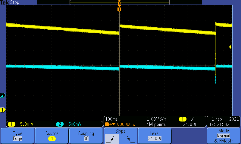
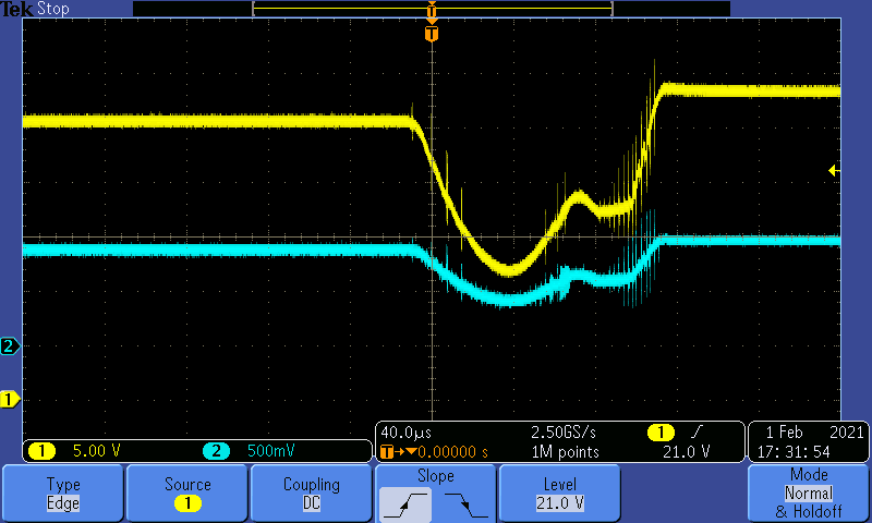
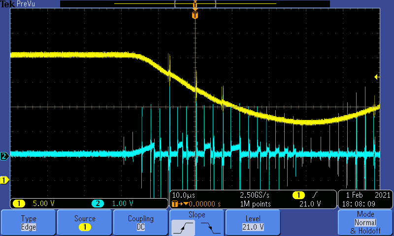
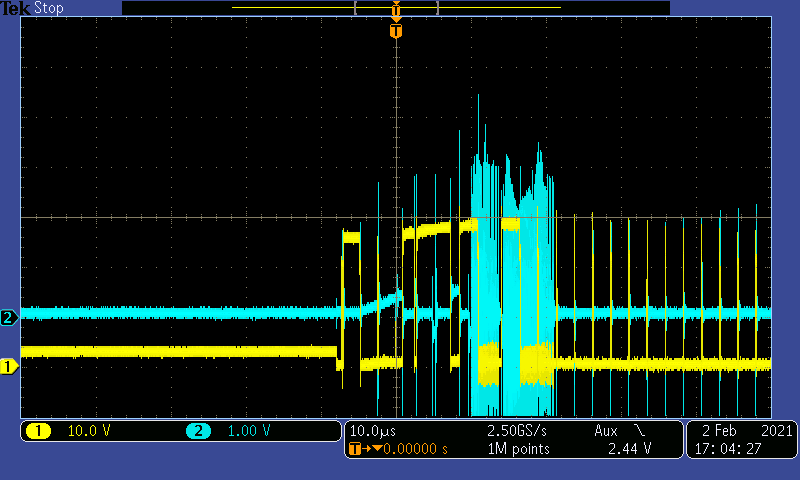
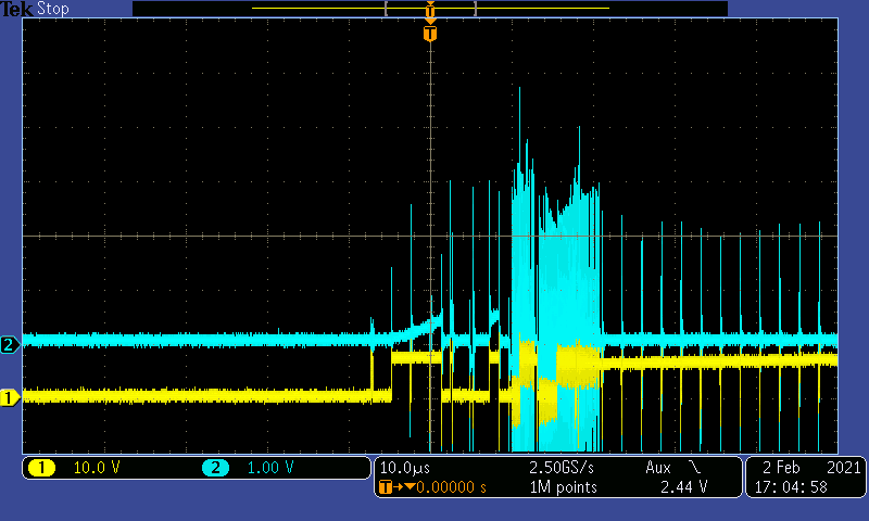
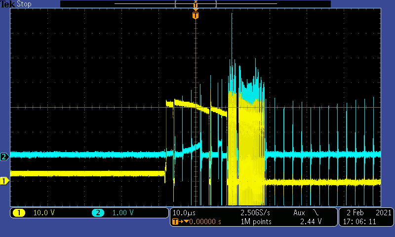
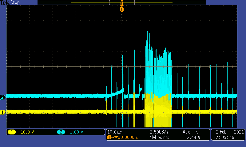
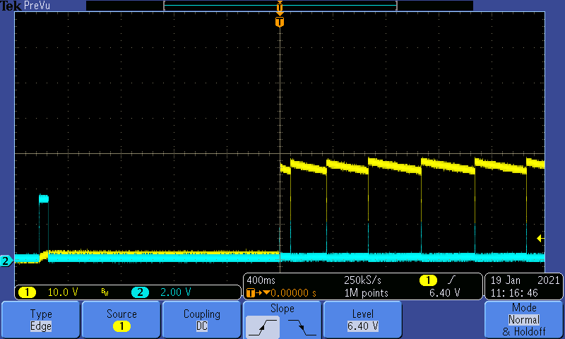
NON-WORKING: Here is what the output voltage (yellow trace) looks like when the unit is powered up from 21V.  The blue trace is the COMP pin.

Can anyone tell me what is going on???  I've verified all my component values, and I've tried various different values for compensation and soft-start.

  • Hello Malcolm,

    Thank you for using LM5175 and I am sorry that it does not perform as you expect it.

    Please let's go on with getting the circuit first to work without the additional voltage setting circuit you have.

    From you description and pictures, I understand that the circuit works when started with an input voltage of 18V, but has issues when starting with 21V. Which load do you have at the output when starting the circuit?

    Here my comments to the schematic:
    - Please remove the capacitor on the RT pin.
    - For 8A output current, you need to reduce the sense resistor to 5 mOhm max. With 7 mOhm you most probable get into current limit at 6A.
    - Remove the capacitors on VISNS and VOSNS and replace the 10 ohm resistor on VOSNS with a short.

    If this does not help, please check the moment when the device shuts down in detail, start with VIN and VOUT next to the IC, the switch nodes, if possible all 4 signals on one scope plot. Then I need to get a more detailed measurement of the COMP pin at the moment when the output shuts down.

    And if you have load on the output, check if the problem is gone when you remove the load.

  • I removed the capacitor from the RT pin.  I removed the capacitors from VISNS and VOSNS and place a jumper across the 10 ohm resistor.  None of this made any difference.

    I have attached all of the scope shots you requested.  I hope this enables some progress.LM5175 Ramping Issue.pdf

  • Hello Malcolm,

    Would you please remove the resistor on MODE and exchange it with a short to VCC? Normally your converter should switch all the time. It is strange that it turns off for a while. Can you please measure the output current when you observe the drop?

  • Brigitte,

    Sorry for the delay, but I got sidelined by other projects.  I hope to be back on this tomorrow.

    Malcolm

  • Hello Malcolm,

    No problem, I hope that we then can solve the issue quickly.

  • I removed R187 and connected the MODE pin directly to VCC.  This made no difference.

    Note there is  no load on the circuit, nor has there been in any of the previous tests.

    By way of review, here is a scope shot of the output waveform (yellow) and the FB waveform (blue):

    Here is an expansion of the trigger point:

    Since there is no load, where is all the energy going when the output plunges to half its value?  There is ~130uF on this output line.  Is it possible that Q39 and Q40 are on simultaneously?

    Also, I keep getting messages from TI Customer Support asking if this issue is resolved.  I thought YOU were customer support.  Do they really not know what is going on?!?

  • In an effort to answer my own question (Where does the energy go?), I took some shot that compare the output voltage to the voltage across R185 (the current sense resistor).  The sense resistor is set to 0.007 ohms.  Here is what I found:

    Buried in the switching transients are pulses that reach almost 0.5V.  That translates into currents of about 70A.  Does that not tell us that both FETs are conducting simultaneously?  Is this normal?

  • In an effort to track down where the energy goes, I took shots that compared the drop across the sense resistor (blue) with the gate signals from each of the switcher MOSFETs (yellow). Since I only have a 2-channel oscilloscope, these are taken in four different shots. Nonetheless, the relationship between the heavy current pulses and the FET gate signals is clear.

    Yellow = gate of Q37 

    Yellow = gate of Q38 

    Yellow = gate of Q39 

    Yellow = gate of Q40 

     The input voltage is set to 19V and it is being boosted to 24V. Under normal operation, Q37 & Q40 should conduct during the first part of the cycle to allow current to build up in the inductor. During the second part of the cycle, Q38 & Q39 should conduct to allow current to flow from ground to the output.

     The pictures appear to show the second half of the cycle where Q38 & Q39 are simultaneously conducting, but the current is flowing backward from the output filter capacitors to ground. Note how the current is ramping upward from zero. (The inductor is 3.3uH, and RDSon of the MOSFETs is 4.2mΩ. The sense resistor is 7mΩ. Thus, the time constant should be about 200uS.)

    Why is the regulator is turning on Q38 & Q39 at a point where the current is already zero?  Shouldn't the soft-start (or some other feature) prevent this?

  • Hello Malcolm,

    When MODE is set to VCC, the converter should switch permanently and never stop switching. I do not understand why the device stops switching at all in your application. Please check PGOOD signal.

    Can you please check the behavior of the output when you reduce the input voltage to possibly 15V or increase it to 32V?

    And just for clarification. You changed the schematic according the recommendations and kept it this way?

  • Brigitte,

    The MODE pin is/was set to VCC and all of the other changes to RT, VISNS and VOSNS are/were still in place.

    Here is the PGOOD signal (blue) along with the output voltage (yellow):

    Here is the same shot showing the detail of the falling edge:

    If I reduce the supply voltage below 17V, the circuit works properly.  Likewise, it works properly if I increase the supply voltage above 31V.

  • Brigitte,

    In combing through the data sheet today, I saw that the SLOPE capacitor is involved in stabilizing the crossover between buck mode and boost mode.  With this in mind, I took some data on the supply voltage range that causes the ramping to occur.  With the present value of 120pF, the ramping occurred at voltages between 20.2V and 30.8V.  When I increased the capacitor to 220pF, the range got significantly larger (16.1V to over 36V).  When I decreased it to 47pF, the problem essentially went away.  This is GOOD news!

    Can you give me some insight into how I should optimize the value of this capacitor?  The value I used came from the WebBench application and it doesn't seem to be correct.

    Malcolm

  • Hello Malcolm,

    Thank you very much for the update. This is great news. Please be aware that the SLOPE capacitor might reduce the VIN range, so please check this with the formulas in chapter 8.3.12 in the datasheet.

    Please have a look into chapter 9.2.2.8 in the datasheet of LM5175 on page 24.

    In addition, this paper might be helpful: 

    But there is the practical aspect, that the right slope compensation is dependent on the used external components, their parasitics and the layout, so it is essential to test this in the application.