


Hi,
I had a few doubts regarding the EVM design and layout/component recommendations for this part, if those could be cleared it would be of great help to finalize my own design with this part:
- In the EVM BOM, the snubber capacitor part is mentioned as "GCM155R71H391KA37D" and its value is noted as 0.39uF. Is it a typo? This part number actually corresponds to 0.39nF ie 390pF (as the datasheet recommends). Also, this part number is different from "GCM1555C1H391JA16" that's recommended in the datasheet but I'm assuming that mostly they are interchangeable.
- Similarly, in the EVM BOM, the snubber resistor part is mentioned as "CRCW08053R90JNEA" as opposed to "CRCW04023R90JNED" that's recommended in the datasheet. Most importantly, the one used on the EVM is a bigger 0805 1/8W one and the datasheet recommended one is a smaller 0402 1/16W one. Which one out of the two is actually the most recommended one to go with?
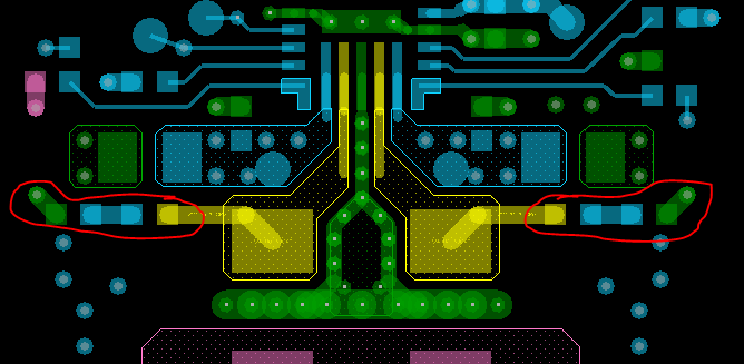
- Is the recommendation to add ground vias even between the 2 pads of the inductors as shown below encircled in green? This is to reduce the EMI radiated?
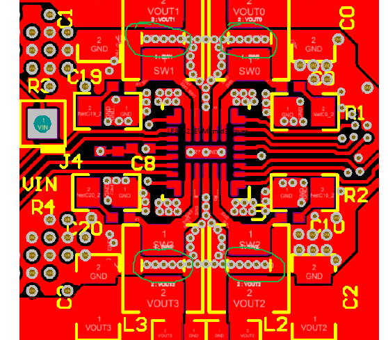
- Does the copper area shape for the SW_Bx nets shown highlighted in yellow below look acceptable from a layout recommendation point of view? Unfortunately, both the recommended inductor parts "DFE252012PD-R47M" (which is a much smaller package, and is the actual one used on the EVM) and "IHLP1616AB-1A" both don't seem to be in stock with the vendors, and I have decided to go ahead with "IHLP1616ABERR47M01" which is the nearest matching one that I could find relative to "IHLP1616AB-1A". Hence the inductor footprint is a bit bigger than the one used in the EVM. From our side we have tried to make the SW_Bx node metal shape area as small as possible but it has to be at least big enough to accommodate the bigger inductor pad as shown highlighted in yellow below. Do you see any concern with this? Also, hope the placement of the snubber RC components as shown encircled in red looks OK as well?

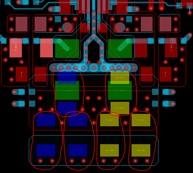
5. As of now I'm placing two 22uF capacitors and an extra DNI cap option as the local bulk VOUT caps per Buck phase as shown encircled in red in the snapshot below. The dark blue shaded caps belong to one particular buck output ie buck phase and the yellow shaded caps to another phase. Since I'm intending to use the buck in 4 phase mode, I'm shorting the outputs together right after the inductors (inductors are shaded in green) using a metal shape as shown below. Is it OK if I keep the capacitors from both phases as near as shown below?
Thanks,
Anoop


