This thread has been locked.

If you have a related question, please click the "Ask a related question" button in the top right corner. The newly created question will be automatically linked to this question.

BQ24170: Input current gradually ramps up to adapter saturation

Part Number: BQ24170

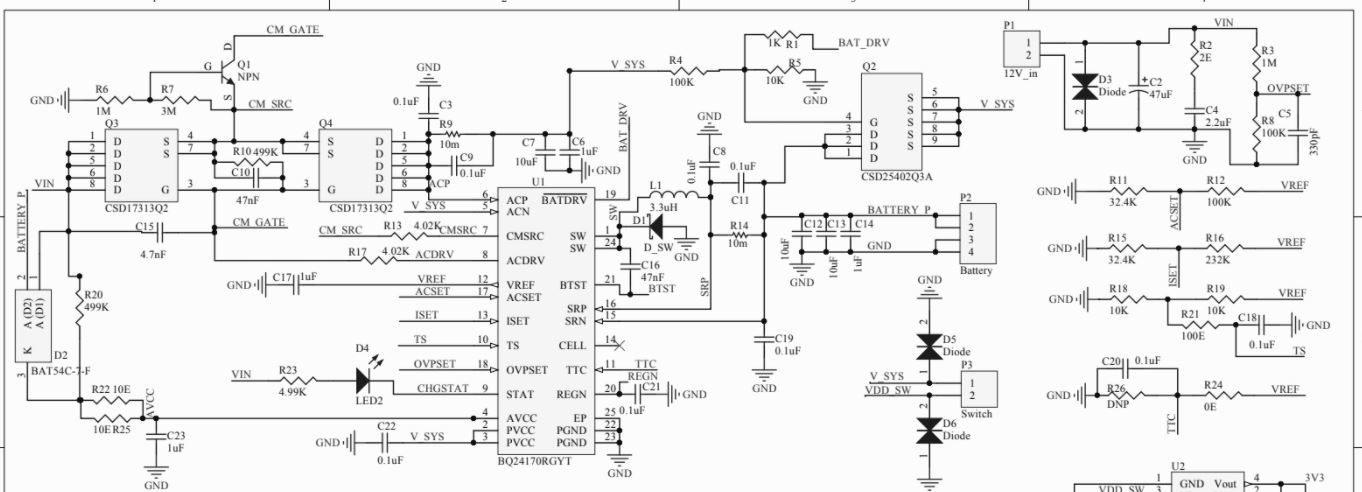
I had posted about this earlier and I had no solution on forums, hence I am trying again. We have designed a PCB for a 2-cell (8.4V max) 2A charging current to charge a 20Ah Li-Ion battery pack (2S8P 18650 pack). We have supplied the input with a 12VDC from a DC power supply capable of supplying upto 3A continuous current. The discharged pack at 7.2V is connected to our PCB and the initial input current is 1.38A. In the exact same setup, the Eval board - BQ24710EVM (which we have purchased and done several tests with) takes 1.35A. This current is stable and will not cross 1.36A till the pack ends up charging 8 hours later. However, in our design, the current slowly ramps up from 1.38A to 1.46A over the first 3 hours, and then abit more quickly. We have had the exact same experience earlier with the same design. We thought we had not followed the layout guidelines to the tee, so we redesigned the PCB by using thick traces, placing components are closed to each other, reducing the loop current area etc. However, we still have the problem. Earlier, we used to assemble the bareboard PCB with a hot air soldering iron. But this time, we outsourced the entire manufacturing process and professionals have assembled the PCB with stencils, pick and place machine and reflow oven. But the problem still persists. I have measured the drop across Rsr (10m) when this happens and the value is not more than 20.4mV. The ACSET value has been set for a IDPM of 4A. The drop across Rac increases propertional with current being sourced from DC power supply. This leads me to believe that the current enters the IC via the PVCC pins and returns via PGND. All reference voltages set are stable (ISET, VOVP, TTC connected to VREF, TS set via voltage divider). Please refer to the schematics. Alot of the resistor and capacitor values have been directly picked from the Eval design schematics. The layout too largely looks similar to the Eval board layout. The SW pin on the IC was probed out on the oscilloscope wrt PGND and we got a 1.65MHz 12Vpp with 65% on-duty cycle wave, which is the same as the eval board. Why is this gradual rise of input current happenening? Can someone help me debug this?

  • Hi Darien,

    I apologize for the delay in response.  We are having weather issues in Dallas, TX, with many of our support team without power or internet.

    To summarize your setup:  VIN=12V, VBATstart=7.2V charging to 8.4V, ACSET=4A, ISET=2A which is constant based on measure of 20.4mV across Rsr=10mohm. On the EVM, with same load/battery attached, you see a steady 1.35A for 3 hours but on your board, you see the current steady increase to 1.46A over 3 hours as the battery charges. 

    1.  If the battery voltage is slowly increasing, I would expect the input current to increase because output power=VBAT*IBAT with VBAT increasing.  Or are you saying that you are holding the battery voltage steady with a battery simulator?

    2.  If you are holding the battery voltage steady, I could explain a small increase in current (less than what you measure) as the IC and/or FETs heat up but I would expect the thermal transient to be much faster than 3 hours.  Did you compare the EVM and your board IC and FET temperatures?  Do you have the IC on your board connected through vias to large ground plane for heat sinking?

    Unrelated question/concern, if ACSET is 4A but input power is 12V @ 3A, is there a concern that the charger will crash the input source.

    Regards,

    Jeff

  • Hi Jeff,

    The PCB that was running away till 3A saturation was damaged since it was tested on a faulty battery, whose internal resistance seemed to be changing with battery voltage. I took another assembled PCB and it works fine. Yes this gradual increase in input current is expected since the output power is increasing as the battery charges up (I realised this now). Our DC power supply has a maximum current safety limit of 3A, but we will change the IDPM to 3A in the next revision so that we can use a lower power adapter. We have connected the BQ24170 GND pad vias to the GND plane. We have made a 4 layer PCB design specifically to deal with GND planes. Thanks so much Jeff for your help.