This thread has been locked.

If you have a related question, please click the "Ask a related question" button in the top right corner. The newly created question will be automatically linked to this question.

UCC21750-Q1: Driving full bridge with UCC21750QDWQ1

Part Number: UCC21750-Q1
Other Parts Discussed in Thread: UCC5390, UCC5350, , UCC21750, UCC21540A-Q1, LMG5200

Hi

Kindly advise me on the following:

1. Are UCC21750QDWQ1/UCC21750QDWRQ1 available in the market or still in prototyping stage?

2. What is the difference between UCC21750QDWQ1 and UCC21750QDWRQ1?

3. The recommended configuration for driving half bridge with two UCC21750QDWQ1 is shown in Fig. 1 as attached (Fig. 50 in the datasheet).

I have six full bridges to drive - containing 24 SiC-MOSFETs (C3M0015065K) . I wish to minimise the I/O of the microcontroller (MCU) as much as possible by using two UCC21750QDWQ1 to drive each full bridge.

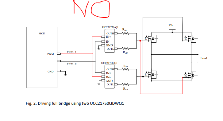
Under this now, I have two questions:

(a) Is it possible to use two UCC21750QDWQ1 to drive full bridge as shown in Fig. 2? if no, is there an alternative configuration?

(b) Still on minimising the I/O of the MCU, if I have a PWM coming from the MCU to the driver as in Fig. 3 and I need to produce its complementary (PWM') (logic inversion), is there any component (IT product) to achieve this?

N.B: If I could achieve (a) and (b), then I'll be able to use two I/Os instead of four (now saving two I/O channels!).

Peradventure I am not channelling my enquiry through the right channel, kindly help me direct it to the appropriate department or personnel. I look forward to getting a response soon. Thank you soon.

Olutayo

Enquiry to Texas - Copy.pdf

  • Hi Olutayo,

    Welcome to E2E!

    I will review these questions and can get back to you by end of week.

    Thank you for your patience.

    Best regards,

    Andy Robles

  • Olutayo Omotoso1 said:

    1. Are UCC21750QDWQ1/UCC21750QDWRQ1 available in the market or still in prototyping stage?

    2. What is the difference between UCC21750QDWQ1 and UCC21750QDWRQ1?

    Yes these products are available for more than 2 years, they are available and in Active status. 

    The difference in those parts is the package they come in . -DWRQ1, the R means tape and reel and moq is 2k because its a massive roll of chips that is used in automated machiens. 

    https://www.ti.com/product/UCC21750-Q1#order-quality

    Look under packaging on the order page for the pkg quantity. If you need less than just a few units u must order DWQ1. You can also order  free samples from this page as well, i think up to 5 per device. If you are not developing for Automotive applications (or any commercial application at all), you can use the non Q1 variant of this part as well. 

    U can also order from digikey or mouser as well if u have other parts u need from there. 

    Olutayo Omotoso1 said:

    3. The recommended configuration for driving half bridge with two UCC21750QDWQ1 is shown in Fig. 1 as attached (Fig. 50 in the datasheet).

    I have six full bridges to drive - containing 24 SiC-MOSFETs (C3M0015065K) . I wish to minimise the I/O of the microcontroller (MCU) as much as possible by using two UCC21750QDWQ1 to drive each full bridge.

    The figure u are showing is have showed an interlocking config. You do not necessarily need interlocking, but absolutely no issues in using it. 

    Olutayo Omotoso1 said:

    (a) Is it possible to use two UCC21750QDWQ1 to drive full bridge as shown in Fig. 2? if no, is there an alternative configuration?

    (b) Still on minimising the I/O of the MCU, if I have a PWM coming from the MCU to the driver as in Fig. 3 and I need to produce its complementary (PWM') (logic inversion), is there any component (IT product) to achieve this?

    N.B: If I could achieve (a) and (b), then I'll be able to use two I/Os instead of four (now saving two I/O channels!).

    You are basically trying to do interlocking with one signal. The main issue is that you MUST ensure adequate deadtime between when top and bottom channels are ON. Otherwise you could get into a situation where top and bottom IGBT/FET are on simulataneously and you short the HV bus to ground. 

    It might be possible but you would have to realllly verify timing / deadtime by calcualtion and ensure enough leeway according to datasheet spec for Pulse width distortion and stuff. You must also consider any delay by the inverter/ buffer. 

    If it can't work , you have no virtually no control over the deadtime without adding some kind of RC filter to the input of your Inverter to explictly add deadtime.

    I really recommend u to avoid doing the inverter method as in fig2/3 as u have limited control and there is a lot of extra variables and unecesary complexity to making the system reliable. 

    Resouces on interlocking / deadtime below: 2nd one will explain the concept of deadtime very well. 

    Another thing to point out, there is a big issue with ur figures 2/3 topology you have proposed. 

    In this configuration, the TOP driver is the highside driver. It is referenced to the source of the top mosfets which moves up and down during operation. 

    Bottmo driver is the low-side driver and referenced to ground and doesn't move. 

    In yoru graph, u have connected the output of ur Highside driver to the lowside of the other half-bridge. Please do not do this. Because the references are different. 

    If your bus voltage is 400V lets say, the Highside driver will going to try to put ~415V on the top gate to achieve VGS=415-400=15V. THis is good .

    However, the Source of the low-side fet is GROUND, so you are effetively putting VGS=415-0V=415V. This is bad. 

    This will probably result in a smoking the low-side FET in a spectacular fashion. The converse is true for the top, youre going to have VSG and VSD >=400V which and smoke those too. 

    You will need have one gate driver per FET for a full-bridge config. 

    Anyways. You can use a rs232 to create a differential signal as well as an alternative to ur inverter solution. 

    Further more if you do not need the Analog to PWM or FAULT signalling back to teh controller you may be able to use UCC5350 or UCC5390. It depends on what youre driving and what ur application needs. 

    If this answers your question please let me know by pressing the green button. 

    Best

    Dimitri

  • Hi Team,

    Thank you so much for providing this explanatory feedback. How about these?

    1. Will the interlocking configuration then be as in Fig 5 of this ref https://e2e.ti.com/support/power-management/f/196/t/967863

    2. Will bootstrap be required in the interlock for the UCC21750Q1 family as shown in Fig. 5 in this ref https://e2e.ti.com/support/power-management/f/196/t/967863 and how are Cboot, Dboot and  Vbiase1 determined?

    Thanks.

  • Olutayo,

    Olutayo Omotoso1 said:

    1. Will the interlocking configuration then be as in Fig 5 of this ref https://e2e.ti.com/support/power-management/f/196/t/967863

    Yes.

    Olutayo Omotoso1 said:

    2. Will bootstrap be required in the interlock for the UCC21750Q1 family as shown in Fig. 5 in this ref https://e2e.ti.com/support/power-management/f/196/t/967863 and how are Cboot, Dboot and  Vbiase1 determined?

    Bootstrap is required if you do not have a seperate Power supply for the highside drivers. As i said before, the Emitter / Source of the Top FETs moves every cycle so teh power supply must float and be seperate from the low side one. 

    So you either need a bootstrap supply or design-in a second isolated supply. Bootstrap is cheaper. 

    https://www.ti.com/lit/an/slua887/slua887.pdf

    This Link ^^^ gives resources on bootstrap component selection. 

    If this answers your question please let me know by pressing the green button. 

    Best

    Dimitri

  • Hi

    Thank you for your responses.

    Still on UCC21750-Q1:

    Please, is there any recommended isolated IC for the input pins (VCC and GND) and output supply pins (VDD-COM-VEE). That is, kindly advise on if there is an isolated IC that can provide 3V to 5V for the input supply (Vcc - GND) and an isolated IC (ICs) that can provide -4V (or near this) to 25V (or near this) for the output supply (VDD - COM-  VEE).

    Regards

    Olutayo.

  • Olutayo, 

    We don't have such power switches that can work at such low VDD, but we may have a solution. 

    What are you driving (P/N helps)

    What frequency?

    What topology ?

    Best

    Dimitri

  • Hi 

    Thank you for the response.

    Please what's P/N?

    I am driving Dual active bridge converter using UCC21750 at <100kHz

    Thanks.

    Olutayo

  • Olatuyo, 

    You can use zener in the driver OUT path with virtually any driver to drop the voltage.

    If you MUST have a low-voltage SUPPLY to the driver your options are more limited. 

    P/n is part numebr. 

    If this is low-voltage, why do you need any isolated driver? 

    Only a few of our isolated devices like UCC21540A-Q1 support 6V or less bias supply. Please note that input supply is different than output so you need to check in the datasheet.  I would suggest looking at our non-isolated devices. If you find a suitable non-isolated driver u can pair it with a seperate isolator. 

    Other solution -> use a lower power buffer (non gate driver) which drives a BJT based push-pull buffer. This topology is actually described in 21750 datasheet iirc. the low voltage buffer doesn't need to sink/source much current, the BJTs current gain takes care of the rest. 

    Your solution may not be supported by "smart' gate drivers like UCC21750 where the minimum VDD is >10V. 

    Maybe a GaN device like lmg5200 could work. 

    Best

    Dimitri