This thread has been locked.

If you have a related question, please click the "Ask a related question" button in the top right corner. The newly created question will be automatically linked to this question.

TPS53647: Schematic Review,OCP Limit and Output Caps

Part Number: TPS53647
Other Parts Discussed in Thread: CSD95490Q5MC,

Hi,

We have completed a design with TPS53647 and 4 Power Stages- CSD95490Q5MC for 0.9V output at 125A.

We will be using TPS53647 in pin strapping mode.

In the datasheet, at page 9 the maximum Imax value is 120A. But in our design we require 125A continuous current. So is it possible to draw 125A current from the output with Imax value set to 120A without triggering the OCP event.

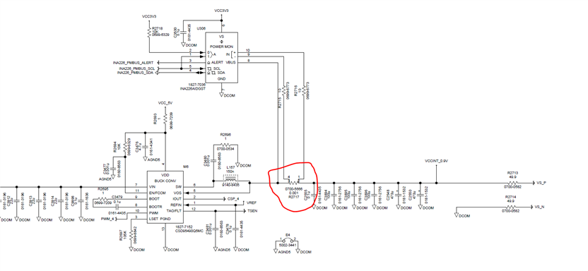
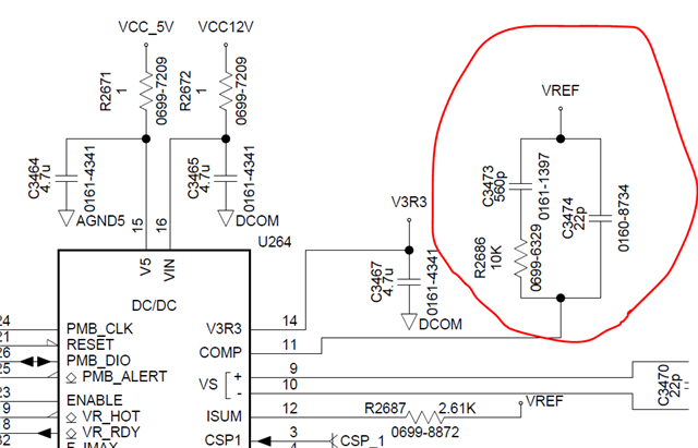
Also, please review the attached schematic for our output requirements.

Please check the pin strap values and also the IMON circuitry and compensation components values for the output requirements.

And one more thing, TPS53647 running at 500Khz and we are using 470uF cap with part no. EEFGX0D471R at the output as this part no. is suggested in the webench simulation also. But when we look at the capacitance vs frequency graph of EEFGX0D471R, we see that at 500kHz the graph doesn't show any capacitance value at 500KHz as shown below:

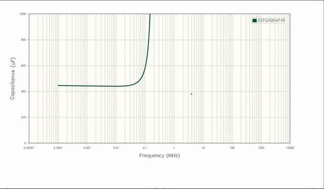
Do we need to choose some other part no. for the output cap and if yes, why it is used in Webench simulation? Please also verify the input and output caps value and quantity.

TPS53647_0V9_125A.pdf

Thanks,

Lalit

  • Hi Lalit-

    1- on the F-IMAX pin, the pin voltage sets the IMAX value, quantized to 8 bits as a fraction of the VREF voltage. So, for 125A, set the pin voltage to appx 0.835V. 

    2- The imon value is for observability. I suggest to set the voltage to appx 100k for 125A. 

    3- This is typical for polymer capacitors. Given the ESR/ESL of each capacitor type, each capacitor type will have a different impedance vs frequency profile. This is why you also need ceramic capacitors at the load side. 

  • Hi Matt,

    Please see the queries on your comments: 

    1- According to datasheet, the maximum IMAX value that can be set is 122A and for that the minimum required voltage is 0.803v. Right now in our schematic, voltage on the F-IMAX pin is set to 0.808v. So, as per your comment ,will increasing the voltage at F-IMAX pin to 0.835v really set the IMAX value to 125A or one can set the IMAX value to maximum 122A as mentioned in the datasheet?

    2- I think controller observes the IMON value to trigger the OCP event if IMAX value which the controller measures with the help of IMON pin exceeds 125% of IMAX.

    Datasheet says to set the voltage at IMON pin to 0.85v for the desired IMAX current.

    Right now IMON value is configured for 122A IMAX current with the help of a 49.9k resistor in parallel with 2.7nf cap from IMON pin to ground.

    So my question here is as datasheet says that OCP event is triggered when the current sensed through IMON pin exceeds 125% of IMAX, which comes out to be ~152A for 122A IMAX value, and as our max output current requirement is 125A only, do we need to change the resistor value from IMON pin to ground or we are good with the 49.9k resistor which is selected for 122A IMAX value.

    Please help on this point as we don't want OCP event to be triggered for our 125A output current requirement.

    3. Our question here is using 470uF(EEFGX0D471R) poly cap here any of use as the cap vs frequency graph attached in the original post doesn't show any capacitance value for 500kHz switching frequency?

    Right now following capacitor are connected at the output of each power stages:

    2x 470uF(Polycap)

    3x 100uF(Ceramic)

    1x 0.1uF(Ceramic)

    Per power stage output current is 31.25A.

    Can you please verify whether we need to modify the quantity or value of the capacitors at the output?


    Also we have one more question on which we need your guidance:

    At the output of one of the power stages, we are using a current sense resistor to measure the current through single power stage and then to calculate the total current from all the four power stages just multiplying the sensed value by 4.

    Can we use this approach of using a current sense resistor with one power stage and the other three will be directly connected to load without any current sense resistor?

    Will there be any variation in the voltage at the output of power stage which uses current sense resistor from the other three which don't use any current sense resistor?

    Please give you thoughts on the above asked questions?

    Thanks,

    Lalit


  • Can we use this approach of using a current sense resistor with one power stage and the other three will be directly connected to load without any current sense resistor?

    Will there be any variation in the voltage at the output of power stage which uses current sense resistor from the other three which don't use any current sense resistor?

    The F-IMAX pin voltage can go from 0V to VREF (1.7V), and it gets quantized to 8 bits, with the full scale value being 256A. The electrical specs table just lists out a couple of options, which will get checked at the final test stage in production. Other values are possible and acceptable. 

    I think controller observes the IMON value to trigger the OCP event if IMAX value which the controller measures with the help of IMON pin exceeds 125% of IMAX.

    Setting the IMAX value to 125A will give an OCP threshold of ~156A. OCP in this device is detected internally by an ADC digitizing the "Isum" value mentioned in the datasheet for the loop. 

    The OCP trigger point does not depend on the IMON pin setting. This language is just recommending that you scale the IMON resistor such that it is 0.85V at full scale. I do not see issues with 49.9k here. 

    3. Our question here is using 470uF(EEFGX0D471R) poly cap here any of use as the cap vs frequency graph attached in the original post doesn't show any capacitance value for 500kHz switching frequency?

    It is normal that bulk capacitors like Poscap/Os-Con/Tantalum/ElCo... do not have much effective capacitance at the switching frequency. Referencing the sketch I pasted before, the bulk capacitors would be the impedance curve listed out in blue. Then the green, red and yellow would be various combinations of local and load-side ceramic bypassing. The combination of all these capacitor types together (as well as the VR gain at lower frequencies below its Fco) gives the output impedance of the converter. 

    In order to tell you if you have enough capacitance or the right mix of MLCC and bulks, I would need to know more about your application. What is the load transient step size, slew rate, and voltage tolerance acceptable to the load?

    Can we use this approach of using a current sense resistor with one power stage and the other three will be directly connected to load without any current sense resistor?

    Will there be any variation in the voltage at the output of power stage which uses current sense resistor from the other three which don't use any current sense resistor?

    This looks OK to me. The controller's current balancing loop will adjust the on-time sent to that one phase, to accomodate the extra votlage drop on it, compared to the other phases. This is conceptually similar to having a mismatched layout between different phases, which is a condition the controller is designed to handle. 

  • Hi Matt,

    Thanks for the quick response.

    Regarding the application of TPS53647 for selecting the output caps:

    We are using TPS53647 for powering the VCCINT supply of Virtex- Ultrascale+ FPGA(XCVU47P).

    We are taking the load transient step size as 62.5A and allowed voltage tolerance is 3% of 0.9v.

    So please check whether the below caps value and quantity per phase are sufficient or not:

    2x 470uF(Polycap)

    3x 100uF(Ceramic)

    1x 0.1uF(Ceramic)

    Thanks,

    Lalit

  • Hello, 

    For a fast slew rate (> VR Bandwidth), you should be OK with 4ph x 2 x 470uF + 4ph  x 3 x 100 uF = ~5mF total capacitance.

    I do recommend to check if Xilinx has any specific recommendations for local bypassing at the BGA, as all that is shown here is VR side capacitors. 

  • Hi Matt,

    Sorry, for the late response.

    Yes we are following Xilinx recommendations for local bypass capacitors.

    I have few more questions for you for finalizing the design:

    1. As discussed previously also, we are using a sense resistor at the o/p of one of the MOSFETs, and you also replied that to accommodate the extra voltage drop controller's current balancing loop will adjust the on-time sent to that one phase.

    My question here is for the above scheme to work do I need to connect the VOS of CSD95490Q5MC after the sense resistor. Right now VOS pin is connected to the output side of the inductor and before the sense resistor?

    2. I am confused about selecting the LSET resistor value. Right now it is 105k in the schematic. Can you please check if this is right value in our design. We are using 150nH inductor.

    3. It will be a great help for us if you can also verify the compensation network values.

    Switching freq is 500KHz and as discussed previously, we are using following capacitor network at the output:

    4ph x 2 x 470uF + 4ph  x 3 x 100 uF

    Compensation components values are : Rcomp = 10k, Ccomps= 560pF and Ccompp = 22pF

    Thanks,

    Lalit

  • Hi Lalit, 

    1- Always connect the VOS pin of the power stage to the output of the inductor. In this case, it should be before the sense resistor. 

    2- Based on the datasheet of CSD95490, LSET =105k is fine for 150nH inductor. 

    3- I have double checked the compensator. This configuration should be stable for power-on.