This thread has been locked.

If you have a related question, please click the "Ask a related question" button in the top right corner. The newly created question will be automatically linked to this question.

TPS53688: Question For The Absolute Maximum Ratings Spec. of SCL and SDA min. = -0.3V

Part Number: TPS53688

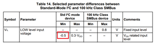
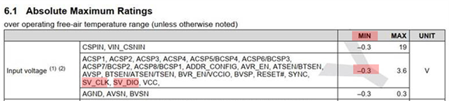
What is the -0.3V voltage unite definition of SCL and SDA absolute rating? Is DC or peak voltage?
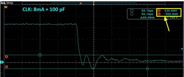
May case as below.

There is a negative ringing happen as SCL signal as -0.56V peak  but data sheet show the absolute min. negative voltage specification is -0,3V.

Note: The signal low level period voltage level is 32mV


  • Hello, this should be an absolute value. You may try to add a series resistor with SCL if there is ringing at the device due to layout parasitics. 

  • Hi Matt,

    Thanks for your feedback.

    BTW, based on the SMBus 3.1 specification.

    It define the VIL min. is -0.5V as below:

    So, may you help to check can the -0.3V be higher if the waveform is just a glitch spike noise?

    BTW, is the -0.3V caused by the body diode of CMOS FET ?

    If it is, Is this glitch spike noise will be damaged the IC ? 

  • Hello, I just want to double check. Are we talking about the PMBus SCL, SDA or the SVID Clock and Data pins?

  • Hi Matt, 

    Yes, we are talking about the PMBus SCL and SDA pins.

    I thought the glitch noise happen at the edge of rising and falling which may caused by below things:

    1. Cross talk phenomenon of PCB Layout

    2. Reflection phenomenon of PCB layout

    Those kind noise energy and spike time were small.

    Based on this concept, I would like to know

    " Will the IC be damaged if the negative spike voltage over the absolute min. -0.3V specification ? " 

  • Hi Jacky,

    First of all I do suggest make sure the measured value is real, but checking it with a differential probe, at the pins of the IC. The waveform may look worse than what the IC actually sees. 

    Exceeding the absolute max specs of the device marginally may not cause catastrophic failure, but it may cause accelerated aging and shifting over time of devices in the IC. We could not make guarantees about this long term. My opinion is that this is "probably" ok given that the duration of exceeding the absolute max rating is only a couple of ns and the lifetime-average duty cycle of exceeding the limit will be extremely small. But as I said before, you may still be able to improve the waveform without any degradation of performance by including a resistor in series with the SCL line. 

  • Hi Matt,

    Thanks for your feedback and I  just summary the key concept as below:

    " Exceeding the absolute max specs of device marginally may not cause catastrophic failure, but it may cause accelerated aging and shifting over time of devices in the IC."

    " TI mention that this glitch noise of -0,56V can be improved by adding a resistor in series with the SCL line."

       BTW, my final two question as below:

    Q1: " Why does not this negative min. specs of device's SCL and SDA  follow the SMBus standard? "

    All MB's SMBus related devices which specs of this negative min. did follow SMBus standard and it is min. -0.5V.

    For example the BMC and CPLD IC.

     Q2: ESD circuit of IC  VS  glitch noise -0.56V  VS The Voltage Unit of Absolute rated min. -0.3VDC

    Based on the website below show the unit is DC voltage of  Absolute rated min. 

    https://e2e.ti.com/support/amplifiers/f/amplifiers-forum/572781/opa172-output-protection

    Based on above description, if the IC do pass the JEDEC JEP-22-C101 related ESD standard.

    The device internal EDS protection TVS diode will act and protect the IC.

    I do understand to add a series resistor can limited the current of glitch noise and prevent to damage the IC's internal TVS diode by current of EOS but not voltage of EOS.

    Just because the TVS diode will be turn on as a forward condition when the glitch negative voltage happen.

    In this case, it is both of current and energy related when the glitch negative voltage happen at TVS diode as froward condition.

    May you  help to confirm my understanding is correct? 

  • Hello,

    1- This device is designed for the SMBus v3.0 high power specifications which do not have a minimum VIL value specified. This table in the post is giving the differences between SMBus/I2C.

    2- The negative bias spec here is based on TI's reliability qualification. Even if the ESD cell is not triggered, it is possible negative bias will cause substrate injection and lead to functional issues. 

  • Hi Matt,

    My boss had below questions:

    1. PMBus ESD cell diode rated forward voltage and current VS PMBus absolute max. rated voltage ( -0.3V min.)

           What is the ESD cell’s diode rated forward voltage and current?

           As below the TPS53688 datasheet, the datasheet show the IOL = -20mA


           Is this 20mA DC also equal to ESD cell's diode rated forward current ?

           Is this 0.3V also equal to ESD cell's diode rated forward voltage ?

    2. HBM ESD Test  (JES-001)  VS All I/O Pins of IC

         Is all I/O pins pass the HBM ESD test and can handle 0.65 A peak to 1.3 A peak ?

    Best Regards

    Jacky Chang

  • Hi Jacky, 

    1- These specs are not about the ESD Diodes, they are giving test limits for the strength (pull-down resistance) of the PMBus Data driver. This is basically saying that when turned ON (E.g. transmitting a data "0"), the TPS53688 Data IO pulls low with a maximum of 0.4V/.02A = 20 Ohms. The value is negative because the device is sinking current through the pull-up resistor during this time. 

    2- All IO pins have passed 2kV HBM ESD qualification on this device. The HBM ESD test basically involves charging a capacitor to 2kV and discharging it into the device through a resistor. The peak current is appx 1.3A, but for a very short amount of time, only 10's of nanoseconds.