This thread has been locked.

If you have a related question, please click the "Ask a related question" button in the top right corner. The newly created question will be automatically linked to this question.

TPS650864: Kindly Review the Schematic of TPS6508641 for timing attached for MPSOC Schematic Design

Part Number: TPS650864
Other Parts Discussed in Thread: TPS544B25, TIDA-01393, TPS650861, TPS548B22, CSD87331Q3D, CSD87381P

For one of our MPSOC (XCZU6CG) based design we have chosen to use TPS6508641

I have strictly followed the user guide and datasheet of TPS6508641

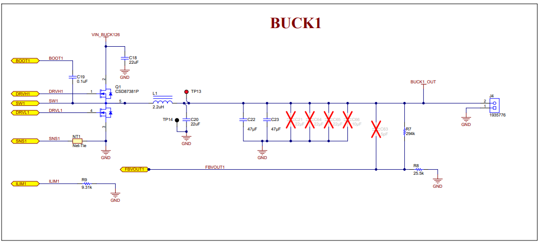
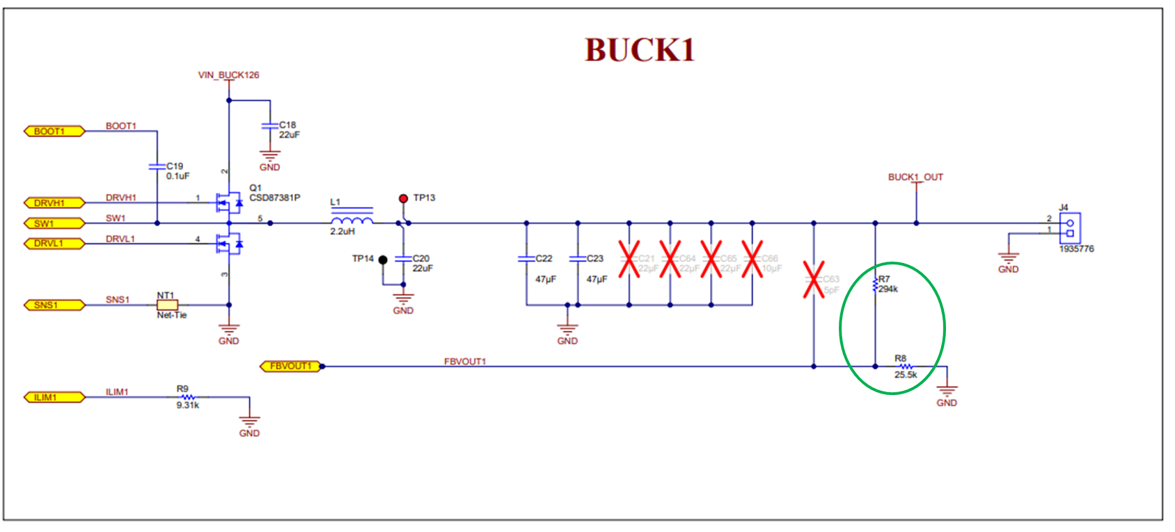
Posted are the Schematic of TPS6508641, for which the timing diagram is also attached

Power_Sequence_MPSOC_XCZU6CG.pdf

SCHEMATIC_PMIC_MPSOC_XCZU6CG.pdf

Kindly let us know whether the schematic will adhere to the timing sequence or not

  • Hi Shyam Daram,

    I am looking over your schematic and will get back with you tomorrow.

    Thank you for your patience,

    Layne J

  • Hi Shyam Daram,

    I have listed some notes below for you to review. 

    1. You must terminate any unused LDOs (in your case LDOA3) with an output capacitor that is connected to ground. If you do not have LDOA3 connected to a capacitor then you will experience a power fault on startup and the device will not complete the sequencing process. We recommend a 4.7uF capacitor for this. 

    2. There is a minimum recommendation of 44uF capacitance on the output of BUCK1/2/6, and we typically recommend using around 100uF capacitance. If you chose to use a lower value around 44uF, you may consider adding some un-populated pads near the other output capacitors in case you need to add more later for better performance. Having more capacitance will improve the ripple on the output of these rails. 

    3. It seems like you are missing a connector that should be between C277, R205, and R204. 

    4. You may already have them on another sheet, but make sure to have pull-ups for the CLK, DATA, and other digital I/O signals you are using.

    Let me know if you have any questions about my comments.

    Best regards,

    Layne J

  • Thanks very much for your detailed points

    In precise i want the timing / sequence to be verified

    Kindly also verify the sequence, will the PMIC perform the sequence provided ?

    the have verified it from Xilinx side for sequence

    Waiting for your Response

    PS: i have made the changes proposed for SCH

  • Hi Shyam Daram,

    Yes the PMIC should sequence as you have specified. The unused rails will still sequence like they are shown to in Figure 6-11 of the TPS6508641 datasheet, but other than those rails your sequencing seems to match the datasheet.

    Best regards,

    Layne J

  • 1. As Suggested, shall i replace the 22uF capacitors i have placed at output of 1/2/6 Bucks with a 100uF ? , kindly suggest the type also , shall i go with a Tantalum type or a MLCC ?

    2. Please Mention the formula to calculate the output voltage of Buck 1

    3. Also please review the upper schematic portion which is  TPS544B25, where it is responsible for generating 0.72V to core supply for a maximum current requirement not exceeding 20A

    I have attached the reference that i generated from WEBENCH tool, i have tried to straight away use the design provided by WEBENCH, still i would like to take your second opinion

    WBDesign136.pdf

    Thanks

  • Hi Shyam Daram,

    1. To clarify my previous comment about output capacitance, we recommend having a total of 100uF of capacitance on the output of BUCK1/2/6. We recommend achieving this by using multiple 22uF or 47uF capacitors in parallel. Refer to the below screenshot of the schematic of TIDA-01393, a TI design using the TPS650864x family of devices. We recommend using ceramic capacitors.

    2. BUCK1 voltage is determined using external feedback. BUCK1 will regulate to keep the voltage on the feedback pin at 0.4V. To achieve a 5V output, we recommend using a resistor divider consisting of one 294k Ohm resistor and one 25.5k Ohm resistor (294k Ohm resistor connected to the output of BUCK1 and 25.5k Ohm resistor connected to ground). 

    3. I have reviewed the TPS544B25 portion of the schematic and I did not find anything obviously wrong with it. However I do not provide support for that specific device and I would recommend making another post specifically regarding that device if you would like a more formal review. 

    Best regards,

    Layne J

  • Thanks for your timely answers

    1. Thanks for the info i shall update my SCH for it

    2. please provide the reference for this in datasheet, unfortunately i could not find it directly in any page, please provide page number / recommended feed back resistors

    3. i have put a alternate thread for this  kindly mark concerned engineer to it

    4. Apart from this if you see the schematic i am not using Buck5, how to terminate un used buck, can i follow the same as done for LDO?, connecting output with a capacitor and leaving feed back path floating, kindly suggest.

    5. What is the need of 0201 shorts referred as Z in the schematic, i have took it as a reference from Ultra96

  • Hi Shyam Daram,

    2. Page 37 of the datasheet lists the settings for the TPS6508641 OTP. There is no specific recommendation in the datasheet for that resistor setup, but it can be found in the schematic for the TIDA-01393 design I linked above. The resistor divider can be seen in the green circle in the screen shot below.

    3. I have referred that thread to the proper team

    4. For this part number you must populate BUCK5 circuitry. BUCK5 Power Good is used to sequence BUCK6 and if BUCK5 is not populated the device will power fault and restart. If you would like to not use BUCK5 you can switch to TPS650861, which is the user programmable version of the TPS650864x devices. The distributor Arrow can also provide pre-programmed units.

    5. That symbol is a net-tie. These can also be found in TIDA-01393.

    Best regards,

    Layne J

  • Layne J said:

    4. For this part number you must populate BUCK5 circuitry. BUCK5 Power Good is used to sequence BUCK6 and if BUCK5 is not populated the device will power fault and restart. If you would like to not use BUCK5 you can switch to TPS650861, which is the user programmable version of the TPS650864x devices. The distributor Arrow can also provide pre-programmed units.

    Layne J

    At this crucial point of time, it will be difficult for me to change the PMIC, just because of one Buck not being used

    is having load compulsory ? or can i leave as shown in schematic but not floating

    In fact i am using the PMIC in always on mode if you see the SCH , does your statement valid for this too ?

    Kindly suggest an alternate way to make Buck 5 reach its PGOOD

  • Hi Shyam Daram,

    Yes it is required to have BUCK5 reach PGOOD, even in always on mode. TPS650861 is the exact same PMIC as TPS6508641. It is pin to pin compatible and the same silicon, however it allows for the user to program it to fit their needs. If changing to TPS650861 is not possible, you do not need to put any load on BUCK5 for PGOOD on BUCK5 to go high. 

    Alternatively, you could switch what BUCK3 and BUCK5 are connected to. In this case you can depopulate BUCK3 circuitry and connect BUCK3 feedback pin (FB3) to the output of BUCK5. This will cause the device to think that BUCK3 has reached output voltage and cause PGOOD for BUCK3 to go high. This works because BUCK3 and BUCK5 are set to use the same output voltage. You need to switch BUCK3 and BUCK5 because BUCK5 sequences before BUCK3. 

    Best regards, 

    Layne J

  • Layne J said:

    Hi Shyam Daram,

    Yes it is required to have BUCK5 reach PGOOD, even in always on mode. TPS650861 is the exact same PMIC as TPS6508641. It is pin to pin compatible and the same silicon, however it allows for the user to program it to fit their needs. If changing to TPS650861 is not possible, you do not need to put any load on BUCK5 for PGOOD on BUCK5 to go high. 

    Alternatively, you could switch what BUCK3 and BUCK5 are connected to. In this case you can depopulate BUCK3 circuitry and connect BUCK3 feedback pin (FB3) to the output of BUCK5. This will cause the device to think that BUCK3 has reached output voltage and cause PGOOD for BUCK3 to go high. This works because BUCK3 and BUCK5 are set to use the same output voltage. You need to switch BUCK3 and BUCK5 because BUCK5 sequences before BUCK3. 

    Best regards, 

    Layne J


    I have took the decision of powering the DDR IC rails with Buck5

    VCCO or the 1.2v of IO lines supply for FPGA will be taken care by Buck3

    This solved my problem

    More over i have few more doubts

    1. Kindly provide Errata of the device , as i want to see any known problems before launching for layout

    2. Also total power dissipation or power consumption calculation of overall IC are required, do i need to use any heatsink if operate the device for worst case temperature of 55 degree centigrade ?

    3. Is there any worst case estimation tool for the device ?

  • Hi Shyam Daram,

    I am looking into your questions and will have an answer for you shortly.

    Best regards,

    Layne J

  • Layne J said:

    Hi Shyam Daram,

    I am looking into your questions and will have an answer for you shortly.

    Best regards,

    Layne J

    Waiting for response

  • Hi Shyam Daram,

    Apologies for the delay. There is not Errata or worst case estimation tool for this device. We do have a power estimation tool that I will share shortly. 

    Best regards,

    Layne J

  • Hi Shyam Daram,

    I have attached the power estimation tool.

    Best regards,

    Layne JTPS65086 Power Estimation Tool with estimated efficiency option.xlsx

  • Thanks Very much, i have few points to say

    1.  Estimation Seems to fail When Buck 4 output is 3.3V, my schematic strictly follows this

    2. Input for 3,4,5 is ok if it is 5V ? or it should be 5.3 ? as default values entered are 5.3 previously

    3. Are On trace test points preferable ? i want to save some space , i want test points for all rails of PMIC, kindly suggest any layout guideline

    4. Attached is the Latest Schematic with replacing the 0.72 source(TPS544B25), as at this thread TI has said the device is not compatible for 0.72 Generation, so i have switched to using a TPS548B22

    Kindly re-look at latest Schematic, i have done all previous changes proposed by you

  • Hi Shyam Daram,

    1. I found a small bug in the back end logic for this spreadsheet. I want to verify my solution for this issue and will post an updated version tomorrow.

    2. Yes a 5V input for those rails is fine. 

    3. What rails are wanting to place test points on? Generally it is up to you for where you would like to place the test points. I would recommend reviewing the reference design using this part, TIDA-01393. Link to the design here.

    4. I will review the schematic soon and give my feedback.

    Best regards,

    Layne J

  • Hi Shyam Daram,

    I have attached the revised version of the power estimation tool. I see you have made all my suggested changes to the schematic. My only comment would be to make sure the I2C pins (CLK and DATA) are pulled up to 1.8V.

    Best regards,

    Layne J

    4162.TPS65086 Power Estimation Tool with estimated efficiency option.xlsx

  • Thanks for the update, i have used it and found my worst case consumption would read to Maximum of 20W at an ambient 55dC

    i have one last doubt, the datasheet of PMIC says it can source up to 7A from Buck1, 2, 6

    I have made my design expecting Maximum worst case consumption of 5A from 1,2,6. The FET which is at the output of the Buck1,2,6 is also good and supports up to 15A

    is there any Disclaimer of using Buck 1,2,6 to their worst scenarios ?

    PS: even the beads i have selected in order to provide noise filtering/ cutting off the rail are infact 100ohm Impedance @ 100Mhz

  • Hi Shyam Daram,

    BUCK1/2/6 will have no issue going to 7A ouptut on the buck controllers (BUCK1/2/6) if the right FETs and inductor are chosen and the input power is able to support it. On page 110 of the TPS650864x datasheet there is a list of FETs we recommend. I would recommend using either CSD87331Q3D or CSD87381P for your specific case. 

    Best regards,

    Layne J