This thread has been locked.

If you have a related question, please click the "Ask a related question" button in the top right corner. The newly created question will be automatically linked to this question.

TPS650864: Kindly Review the Schematic of TPS650864 for 0.72V core voltage generation of WEBENCH

Part Number: TPS650864
Other Parts Discussed in Thread: TPS544B25, TPS543B20, TPS56221, TPS548B22

In the this thread i have got my PMIC schematic for MPSOC reviewed, imporatantly TPS650864 is used in this schematic for 0.72 core voltage generation

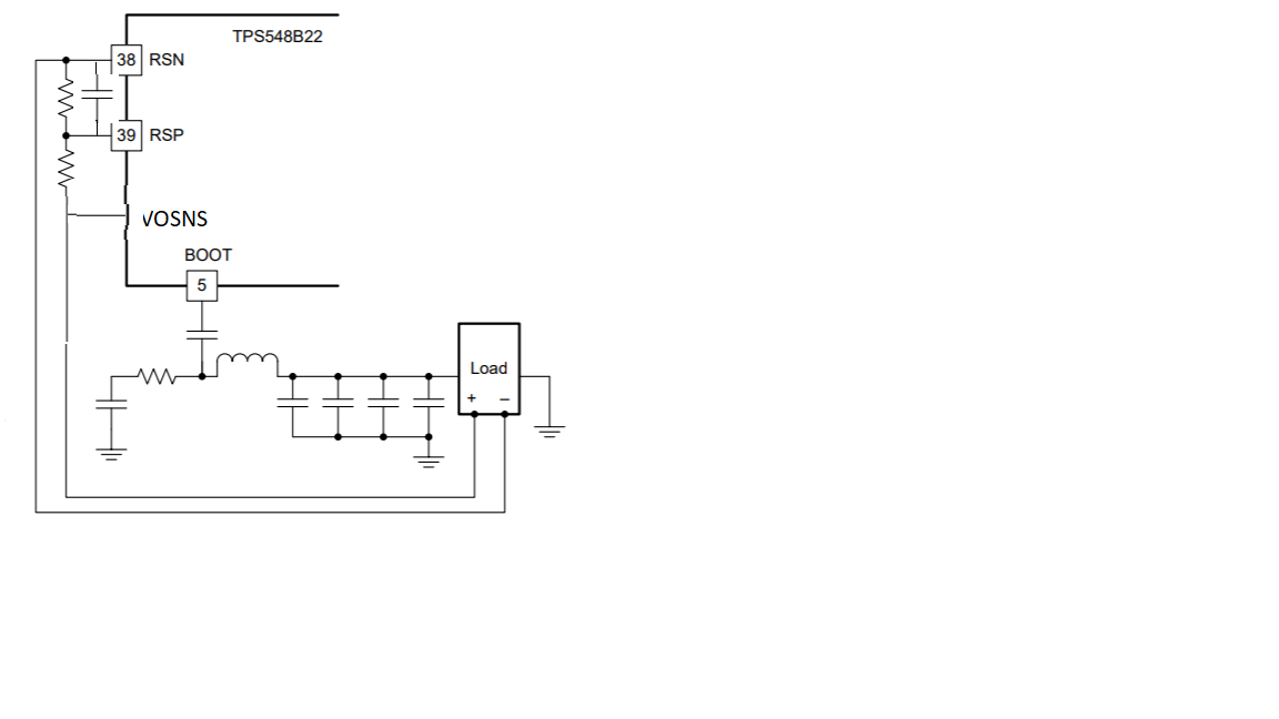
I have attached the reference that i generated from WEBENCH tool, i have tried to straight away use the design provided by WEBENCH, still i would like to take your second opinion

8004.SCHEMATIC_PMIC_MPSOC_XCZU6CG.pdf

5584.WBDesign136.pdf

Kindly review

  • TI, I am Waiting for a response

    Kindly have a look

  • Hi Shyam

        To help with the schematic review, can you please update the schematic for TPS544B25 with the voltage rating of capacitors? 

    Regards,

    Gerold

  • Gerold Dhanabalan - Online Design Tools said:

    Hi Shyam

        To help with the schematic review, can you please update the schematic for TPS544B25 with the voltage rating of capacitors? 

    Regards,

    Gerold

    The Generated Schematic from WEBENCH is as it is followed, the attachment of WEBENCH design contains voltage ratings MPN everything

  • Waiting for response

    Thanks

  • Hi Shyam

      Here is some feedback.

    1. Looks like you are not using PMBUS to set the outpt voltage. This means that you will have to use the feedback divider network to appropriately set Vout without which you will not have output voltage set to 0.72V. 

    2. add an extra 100nf of cap on bp6 (with appropriate voltage rating) for high frequency noise filtering.


    3. The 47uF capacitor at the output should be X5R or X7R or better. It should not be X6S.

    4. the boot resistor value of 100mohm value could be larger. You can leave it as a place holder for now.

    5. Some of the resistor recommended by WEBENCH are 0201. If that is too small for your flow, please use 0402 instead of 0201.

    This is a PMBUS device and you dont seem to be using the functionality. Any specific reason you have chosen this device?

    Regards,

    Gerold

  • 1. True I am not using any PMBUS, i rely on feedback divider CKT for generating 0.72V, isnt the CKT attached following it ?, if not kindly help in choosing the necessary feedback divider

    2. Noted and SCH modified accordingly

    3. Noted will take care

    4. How much larger ? 1 Ohm ? or 10Ohm kindly suggest, so that i can carry a backup

    5. Noted, i shall stick to 0402 Only

    6. I have no special reason to choose this device, it is as per suggestion in section 6.3 of 

    Thanks

    Will be waiting for your reply, i have to launch my design this week

  • Hi Shyam,

        Its a little tricky to get this device to boot to 0.72V without using PMBUS. Can you please send me your detailed requirements? We will recommend the right product.

    Vinmin, Vinmax, Vout, Ioutmax

    Vout accuracy requirements, Load transient requirements

    Any specific feature needed (e.g. SYNC pin etc.)

  • 1. The references of TI mostly suggest in using B/C variant of TPS544x25, and the literature no where mentions that PM bus is must  example1 , example2

    Kindly explain this first.

    2. i need a exact replacement of device TPS544x25 as it adheres to characteristics required

    3. Yet if 1,2 are not explainable here are the parameters

    Vinmin=10v, Vinmax=14v these would come from a 28V to 12V converter DCDC,

    Vout =0.72v,Accuracy is a key parameter which is +/- 0.02v in other words Max ripple 2%

    Ioutmax = 20A, Iout nominal 12A, i could not find the transient conditions from xilinx literature but one of the TI reference is speaking on it (Info on Transient Load )

    4. Importantly i want to tie the LDO3P3 of PMIC to Enable of 0.72v dcdc so that it boots first , so a Enable pin is must , for sequencing i need  PGOOD pin from 0.72v dcdc

    Kindly re look in to my choice of using TPS544x25, as its suggested by many TI documentations and development boards

  • Hi Shyam,

      If you download the schematics file, you can find the PMBUS connector to program the device using a separate USB-2-GPIO hardware.

    http://www.ti.com/tool/PMP12004-HE?keyMatch=PMP12004&tisearch=Search-EN-everything&usecase=part-number

    The issue is because of Vout of 0.72V because the minimum reference on the device is 0.8V without using PMBUS. With PMBUS I can achieve  low as 0.5V.

    Our recommendation for a device without PMBUS would be the TPS543B20 that can help you meet your requirements.

    Please let us know if you have more questions.

    Regards,

    Gerold

  • Very Thanks for your detailed clarification, i shall not use current device

    Coming to usage of TPS543B20 ,

    I have constrainted on board size requirements

    a short search on webench gives me a suggestion to use TPS56221 which shows better efficiency and footprint size of just 400mm2

    where as your suggestion at same efficiency is double the area covered

    Kindly comment on usage of TPS56221 for Ultrascale devices

  • Hi Shyam,

         The TPS56221 does not have remote sense. For these high currents and given the accuracy requirements, it might be good to have remote sense.

    Here is another design using the TPS548B22.  I tried to optimize the WEBENCH design to meet your transient requirements. This capability will be released for this device on the tool in a couple of weeks. In the meantime I tried to optimize it using an internal version of the tool.

    You can scroll to the operating values section of the pdf and see that the Vout ripple, Vout over/undershoot are well within the specs.

    You can add a couple of place holders in the schematic for some caps such as 2x47uF, 2x1uF caps as well to minimize any noise peaks due to resonance.

    Regards,

    Gerold

    WBDesign10752.pdf

  • Here is the Full Schematic of my updated design using TPS548B22 and PMIC, kindly review for Power Good and Wakeup of tps548b22

    One thing i feel is, it kills plenty of space, is there a way i can reduce ? over all area shown by tool is around 800mm2

  • Waiting for response for updated design upload,

    Kindly respond

  • Hi Shyam,

        Here is the feedback.

    1. For Vout, add 1X47uF  and 1x10uF and 1x1uF and 1X0.1uF ceramic capacitor as part of the output capacitor bank – to ensure that there are not gaps due to self resonances. 

    2. Add a 10 ohm resistor between Vout and RSP. 

    3. Add a 10 ohm resistor between GND and RSN.

    4. Add a 1nf cap between RSP and RSN. This 10ohm-1nF-10ohm structure will serve as a filter.

    5. Ensure that the resistors for MODE, VSEL, FSEL are 1% tolerance or better.

    6. Add a 0402, 2 ohm boot resistor in series with the boot capacitor

    7. Add a snubber of 1ohm (0805) and 1nF capacitor (50V rated) between the SW node to ground.

    8. Change the VDD capacitance as below

    Use a 4.7uF, X5R, 25V or 50V rated ceramic cap (the voltage rating can depend on the Vinmax for your application). The minimum effective capacitance should be more than 1uF.

    Use two 2.2nF, X5R, 25V or 50V rated cap ((the voltage rating can depend on the Vinmax for your application).

    9. Check that the BP capacitor is rated 16V or above - if you are using 25V, thats fine. 

    10. Also, it might be good to  have 3 separate symbols for AGND, DRGND and PGND and they should all be connected together on the layout - follow layout instructions closely - this is very important.

    11. The other plate of the BP capacitor should be connected to DRGND ONLY.

    12. The bottom plate of the 4.7uF and 2.2nF capacitors for VDD should be connected to DRGND ONLY.

    13. The bottom resistor on FSEL,VSEL, MODE pins should be connected to AGND ONLY.

    14. The RILIM resistor should be connected to AGND ONLY.

    Please follow layout guidelines in the datasheet.

    Regards,

    Gerold

  • Thanks very much for your detailed review

    I have done all modifications suggested, please find the attachment and give final comments

    my only doubt is, the datasheet says a 1uF cap between AGND and VDD is enough, the reference board has caps with reference to DRND

    please resolve the confusion

  • Hi Shyam,

         You can connect the 4.7uF cap between VDD and DRGND ( I will correct my early statement about connecting it to AGND). In this specific device, you should connect DRGND to thermal pad using a short trace. Connect the AGND to thermal pad using a short trace. 

    From the datasheet mentioning connection to AGND, as the AGND and DRGND pins are close to each that the difference may not be much - but still better to connect the lower plate of the capacitor to DRGND. 

    The snubber capacitor should be connected to PGND. The snubber resistor should be atleast 250mW rated.

    It might be good to add an additionl 22uF at the input PVIN (just in case you need it)

    Given the feedback divider network, you can remove the R348, R359 10ohm resistors.

    the value of the Cfilter C291 can be determined by the following equation.

    C = 1 / [ 2 * pi() * 1 / ( 1/R1 + 1/R2) * Fbw ]


                    R1 = VOSNS to RSP

                    R2 = RSP to RSN

                    Fbw = 2-5 MHz

    The connection would be as below.

    Regards,

    Gerold

  • Hope i can go to fabrication with the above Final Schematic

    i used 220E for R1,R2 and C291 to 22uF, VOSNS to ouput, RSN to GND as suggested

    Kindly confirm

  • Hi Shyam,

        The snubber capacitor is C286 and should be connected to PGND and NOT the RSP pin.

    You dont need R425 and R424.

    22uF for C291 looks pretty high - did you calculate using the formula that was given?

    regards,

    Gerold

  • I shall change the snubber accordinly,

    From the formula given above,  making R1,R2 as same that is 220E will result a Capacitance of 22uF at 2-5Mhz frequency

    now you are saying R1,R2 from above formula are not required

    Kindly explain

  • Hi Shyam,

       In your application, R1 = 100k and R2=49.9k. 

    If you use these in the formula, then Cfilt comes to 2.39pF. Use the value closest to this.

    Regards,

    Gerold