This thread has been locked.
If you have a related question, please click the "Ask a related question" button in the top right corner. The newly created question will be automatically linked to this question.
My last thread: BQ77915: My PCB is not work. - Power management forum - Power management - TI E2E support forums
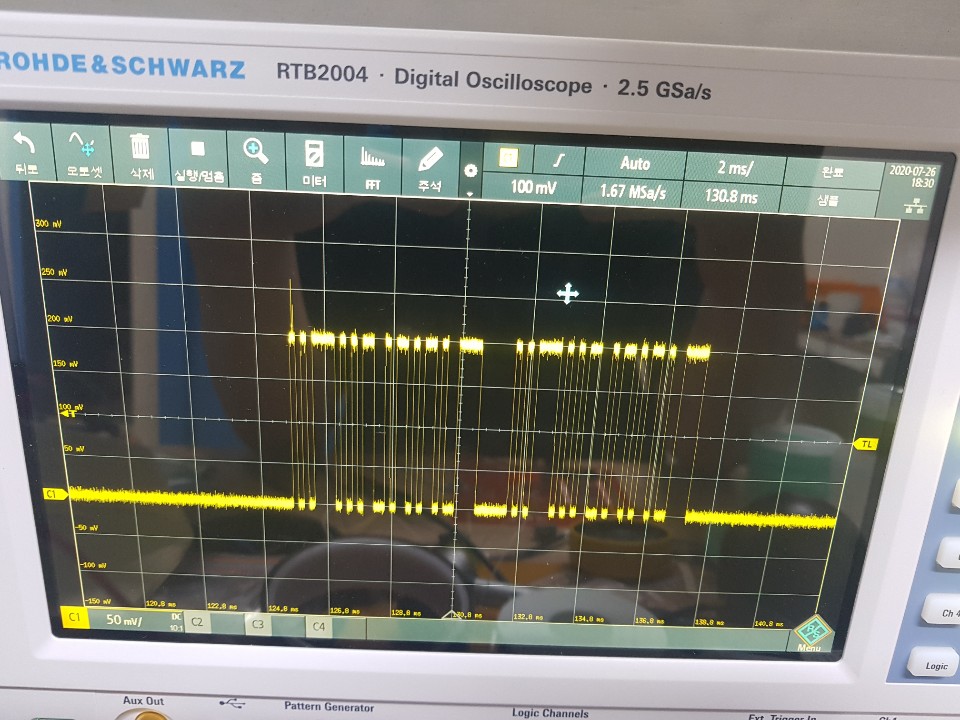
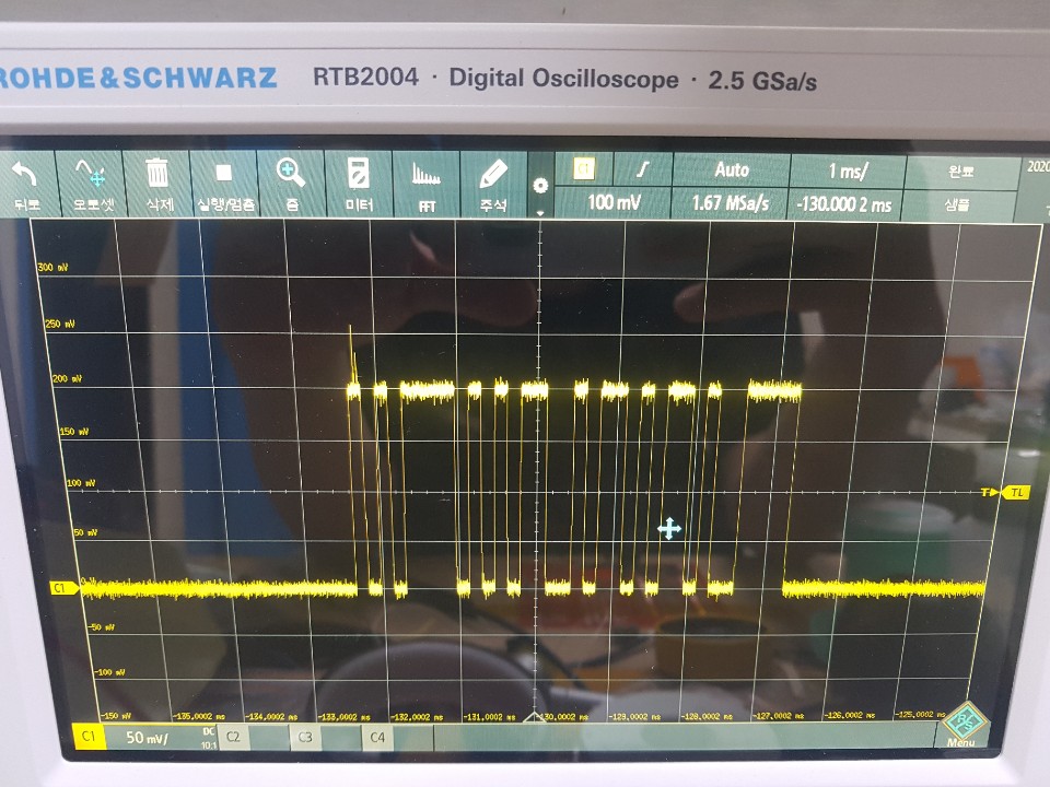
I tried to fix my circuit with my equipment, PSU, and Oscilloscope.
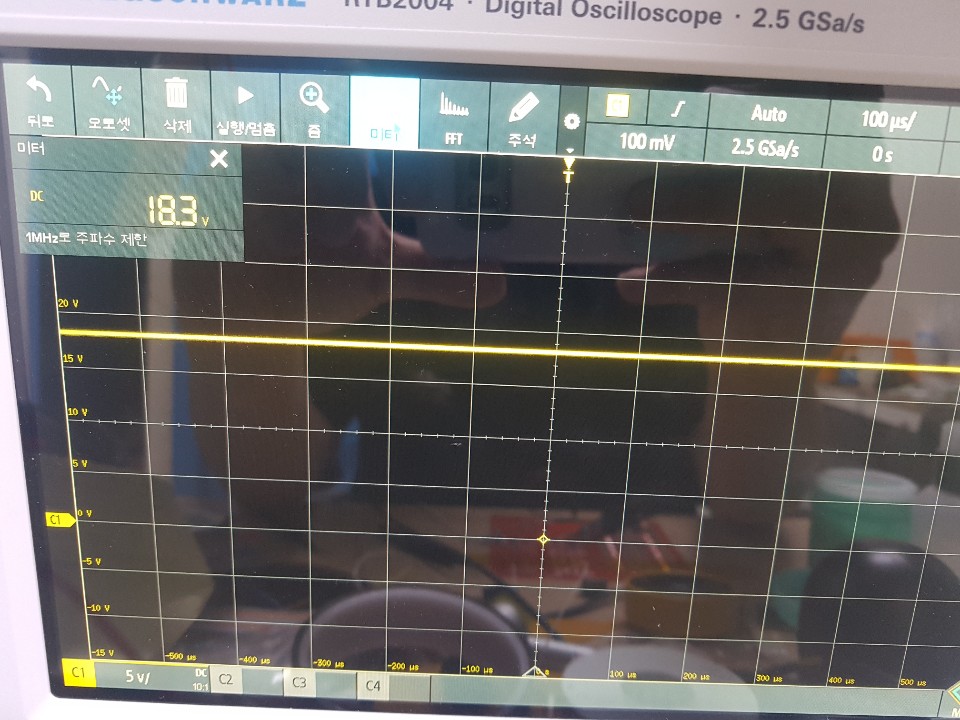
I supply 18V via PSU with 200Ohm Resistor each one to 5S.
Also, I make circuits for Disable Hibernate mode and CTRD, CTRC for ground.
And I used OCDP resistor 100Kohm for using the EEPROM setting.
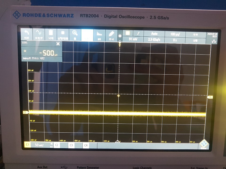
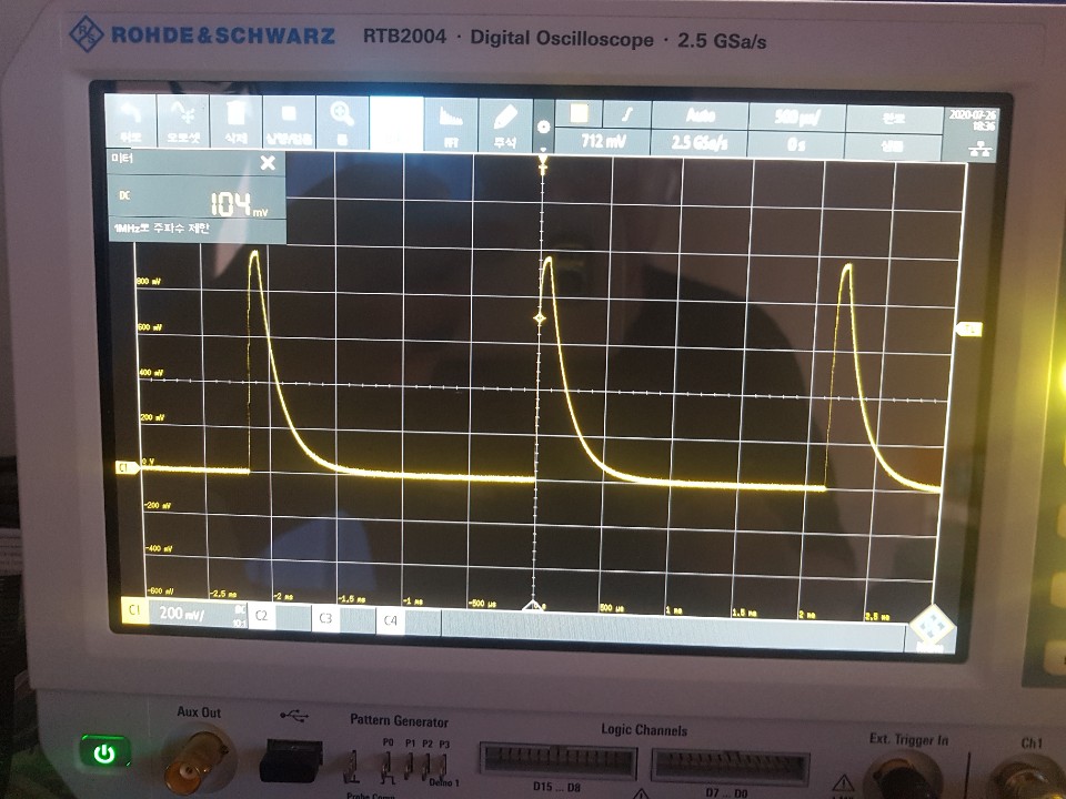
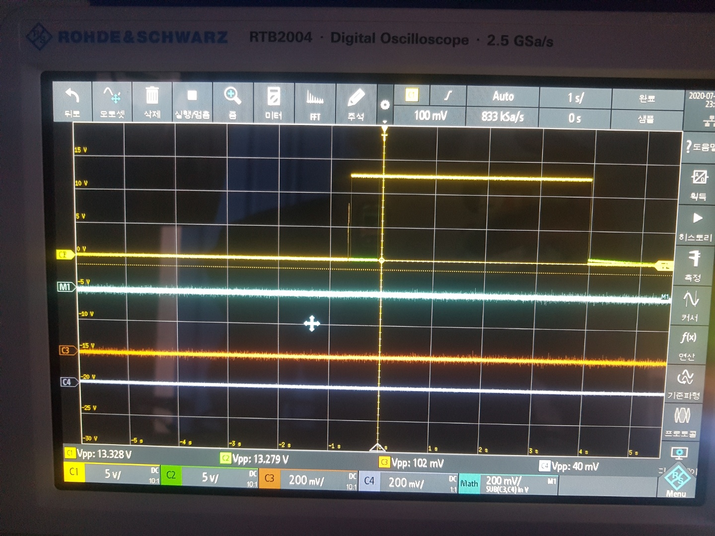
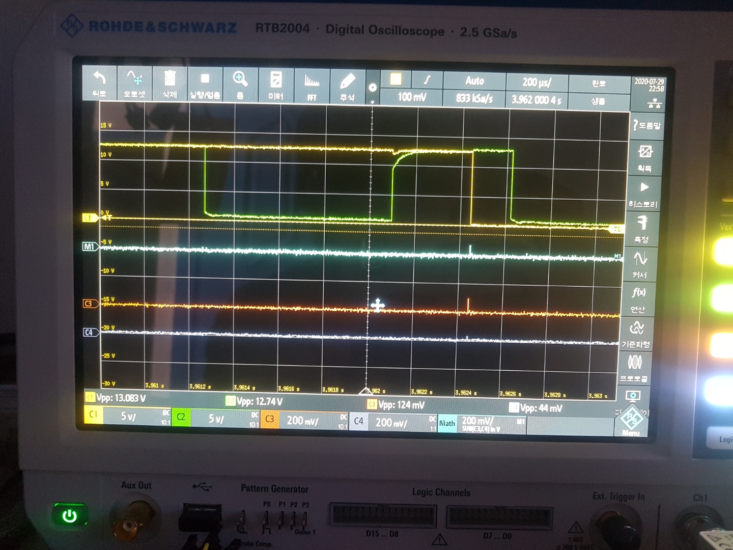
But I can't get Voltage 18V via P- and C5.
I can get only around 16V on P- and FETs' Drain voltage between C5 and Drain 1.6V~3V.
RSNS : 0.002R 1% 3920
MOSFET : FDBL86066-F085(CHG and DSG each 2pcs)
Attach my measurements.
1. EEPROM measurement
2 - 1 - 1 - 1 - 2
Idk what protocol about this, but it seems to be this.
two messages on first time
one message on 2, 3, and 4
and return to first message.
Voltage is 0.3V and looks like for communication from IC.
2. PRES measurement
I added 100Kohm resistor between PRES and VDD.
3. LD measurement
I measured IC's LD pin.
Idk how can I analyze this.
4. VTB and TS measurements
I think this is work well becuz I added pull up resistor, 10K, between VTB and TS
5. DSG_IC and CHG_IC(Output by IC) measurements
It looks like not work.
I saw on datasheet that when PSU supply 18V and if using 200R voltage divider, all FETs are ON
But I can get only around 50mV each Gate.
Even I measured on FET side, it looks same.
6. CCFG measurement
Idk how can I analyze this measurement result.
Hi,
It looks like both the CHG and DSG pin are low, which means there is either a open wire, over current, short circuit, or a temperature fault. Please check the conditions of these faults, found in table 9-5 of the datasheet.
I also noticed the CCFG pin does not look correct. If you are using a 4 cell configuration, the CCFG pin should be tied directly to AVDD (which should be high).
My cell config is 5S during the test.
I supplied to PCB 18V with 200R resistors for dividing voltage to each VC pins.
I attach more measurements that when I powered up my PSU.
This is when I powered up my PSU can getting my SINGLE function.
I can see DSG FET's gate is high to 13V.
Also sometimes later. CHG FET's gate also becomes high.
but ALL FETS' gate was getting low even I didn't load this circuit.
YELLO : DSG FET GATE
GREEN : CHG FET GATE
ORANGE : SRP
BLUE : SRN
SKY : SRP-SRN
even I checked datasheet about CCFG, but 5S just have to float them.
Also, I checked all of the table 9-5. I think I don't have any correspond to them.
How can I analyze my measurements attached to here?
VTB and TS , CCFG , LD , DSG and CHG.
Thank you.
Hi,
Table 9-5 is going to be the key to debugging your board. First, I would recommend determining the values of the CHG and DSG pins. If both pins are high, there is no fault and your device is operating normally. If either, or both, of these pins is high, use the table to determine which faults could be happening.
Then, once you have determined the possible faults, check the fault trigger conditions until you determine which fault is occurring.
Finally, use the the recovery method to return the device to normal mode.