


Part Number: TDA4VM
Team,
Could you please help with the below?
Goal is to configure two PCIe modules to access each other.
In this regard, I’ve noticed that I have a lack in understanding how the interconnect of SoC works in detail. I think I’m missing here the bigger picture.
Up to now, it was sufficient for me to look at the TRM Memory Map of a specific module of interest, to access it functionality via emulator/processor.
For example, GPIO0 module of main domain:
Now I am confronted with a more complex PCIe module: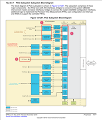
There are now some new terms for me, which I am not sure how they fit into “the bigger picture”:
Q1: What exactly is the CBASS?
Q2: What is VBUS(M/P)? How does it correlate to CBASS?
Q3: Why has the PCIe module internal AXI ports (marked with (1) ) ?
Q4: If CBASS, VBUS(M/P) and AXI are different busses, do they use different addresses to access the same peripheral (marked with (2))?
Q5: Given the memory map for PCIE0_DAT0: Is this address a CBASS, VBUS(M/P) or AXI address?
Q6: What is the “AXI Stream” (marked with (3))?
Thanks in advance!
