


Hi experts,
Please let me confirm about the power down sequence.
In the datasheet "6.3.2 Power-Down Sequence", it is stated that the power down sequence request is the reverse of the power up request (6.3.1 Power-Supply Sequencing). From this, we understand that the falling edge of the power supply must satisfy either of the following:
(1) DVDD15 ->DVDD18 -> CVDD1 -> CVDD
(2) DVDD15 -> CVDD1 -> CVDD -> DVDD18
The customer created a board using C6657 and checked the Power-Down Sequence, and the waveform was as follows.
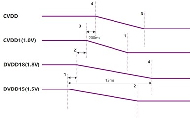
- The timing of the start of the falling edge satisfies (1). (The falling edge starts in the order of (1) at an interval of about 200ns.
- The timing at which each power supply reaches the lower limit of the recommended operating range is CVDD1 -> CVDD -> DVDD15=DVDD18, which does not meet the above regulation. (The above diagram is just an image and the actual waveform is as shown in this text.)
- The timing at which each power supply becomes 0V is CVDD1 -> DVDD15 -> CVDD -> DVDD18, which does not meet the above regulation.
- All power supplies reach 0V within 13ms.
Question 1: Which of the following applies to the Power-Down Sequence explained above?
- There is no problem because the timing of the start of falling edge satisfies (1).
- There is no problem because all power supplies reach 0V within 13ms, although it is hard to say that it meets the requirement.
- There is a problem because it is not recommended in the datasheet.
Question 2: If the answer to question 1 is "there is a problem", is the following guess correct?
- The current consumption increases when the power is turned off, but the device is not damaged. (It is possible to use the device as it is if there are sufficient heat generation measures and power supply capacity.)
- There is a possibility that the life of the device will be shortened.
- There is a possibility that the device will be damaged.
I asked this question because I couldn't decide whether the Power-Down Sequence like this waveform is a problem or not.
Best Regards,
O.H
