


Part Number: AM5729
Hi Team,
we are tested GPIO togging with the help of JTAG debug. we tried to test SD card bootup method. DDR is not up when we use SD card. please give proper steps for MLO creation and SD Card bootup for our Custom board AM5729.

This thread has been locked.
If you have a related question, please click the "Ask a related question" button in the top right corner. The newly created question will be automatically linked to this question.
Part Number: AM5729
Hi Team,
we are tested GPIO togging with the help of JTAG debug. we tried to test SD card bootup method. DDR is not up when we use SD card. please give proper steps for MLO creation and SD Card bootup for our Custom board AM5729.
Hi,
Are you able to configure the DDR configuration through CCS?
If so, then you must know the CCS flow. It will load all the configuration through gel files. So, now if you want to use SD/QSPI, you have to update the same configuration as gel to MLO. For make it easy, note down all the changes you have done in gel files and replicate that in respective board library. Then build the board library so that board/lib get updated with new changes. And then build the MLO. For building MLO, Please check below command to execute from pdk/packages folder - gmake -C ti/boot/sbl all BOARD=idkAM572x SOC=AM572x BOOTMODE=mmcsd .

Thanks for reply Anubhav.
Note: we need steps for RTOS, not using linux.
We did below modification/changes in gel file.
1. Since we are not using EMIF2, we did #deine IS_EMIF2_AVAILABLE 0U.
2. Replaced emif tool generated sbl gel into AM572x_set_emif1_params_dd3_532(uint32_t base_addr) function in gel file.
3. Replaced emif tool generated dmm_lisa_map_regs in register values(U-BOOT) into AM572x_set_lisa_maps() function in gel file.
where to mention this in board library for generating of MLO file?
we did some modification based on our knowledge inn ddr.c file.
1. We copied only below information in ddr.c file
SDRAM_TIM_1 = 0xCEEF36EBU;
SDRAM_TIM_2 = 0x308F7FDAU;
SDRAM_TIM_3 = 0x407F88A8U;
SDRAM_REF_CTRL = 0x00001035U;
SDRAM_REF_CTRL_INIT = 0x000040F1U;
SDRAM_CONFIG = 0x618512B2U;
EMIF_PHY_READ_LATENCY = 0xAU;
EMIF_PHY_INVERT_CLKOUT = 0x1U;
EMIF_PHY_HALF_DELAY_MODE = 0x1U;
EMIF_PHY_DQ_OFFSET = 0x40U;
EMIF_PHY_CTRL_SLAVE_RATIO = 0x80U;
DISABLE_READ_LEVELING = 0x0U;
DISABLE_READ_GATE_LEVELING = 0x0U;
DISABLE_WRITE_LEVELING = 0x0U;
we have some other info also be in emif tools register values, those information we didn't add it in ddr.c file but we added in gel file. If i need to add these lines also be in ddr.c file, where to add it.
/* EXT_PHY_CTRL_xx are used only in case of HW_LEVELING_ENABLED = 0*/
/* EMIF_PHY_FIFO_WE_SLAVE_RATIO (RD_DQS_GATE) */
EXT_PHY_CTRL_2 = 0x006B0088U;
EXT_PHY_CTRL_3 = 0x006B0089U;
EXT_PHY_CTRL_4 = 0x006B007EU;
EXT_PHY_CTRL_5 = 0x006B007FU;
EXT_PHY_CTRL_6 = 0x006B006BU;
/* EMIF_PHY_RD_DQS_SLAVE_RATIO */
EXT_PHY_CTRL_7 = 0x00320032U;
EXT_PHY_CTRL_8 = 0x00320032U;
EXT_PHY_CTRL_9 = 0x00320032U;
EXT_PHY_CTRL_10 = 0x00320032U;
EXT_PHY_CTRL_11 = 0x00320032U;
/* EMIF_PHY_WR_DQS_SLAVE_RATIO */
EXT_PHY_CTRL_17 = 0x00400048U;
EXT_PHY_CTRL_18 = 0x00400048U;
EXT_PHY_CTRL_19 = 0x0040003AU;
EXT_PHY_CTRL_20 = 0x00400039U;
EXT_PHY_CTRL_21 = 0x00400040U;
for your reference attached emif tool spreadsheet and ddr.c file.
EMIF_RegisterConfig_new.xlsm
/******************************************************************************
 * Copyright (c) 2010-2015 Texas Instruments Incorporated - http://www.ti.com
 *
 *  Redistribution and use in source and binary forms, with or without
 *  modification, are permitted provided that the following conditions
 *  are met:
 *
 *    Redistributions of source code must retain the above copyright
 *    notice, this list of conditions and the following disclaimer.
 *
 *    Redistributions in binary form must reproduce the above copyright
 *    notice, this list of conditions and the following disclaimer in the
 *    documentation and/or other materials provided with the
 *    distribution.
 *
 *    Neither the name of Texas Instruments Incorporated nor the names of
 *    its contributors may be used to endorse or promote products derived
 *    from this software without specific prior written permission.
 *
 *  THIS SOFTWARE IS PROVIDED BY THE COPYRIGHT HOLDERS AND CONTRIBUTORS
 *  "AS IS" AND ANY EXPRESS OR IMPLIED WARRANTIES, INCLUDING, BUT NOT
 *  LIMITED TO, THE IMPLIED WARRANTIES OF MERCHANTABILITY AND FITNESS FOR
 *  A PARTICULAR PURPOSE ARE DISCLAIMED. IN NO EVENT SHALL THE COPYRIGHT
 *  OWNER OR CONTRIBUTORS BE LIABLE FOR ANY DIRECT, INDIRECT, INCIDENTAL,
 *  SPECIAL, EXEMPLARY, OR CONSEQUENTIAL DAMAGES (INCLUDING, BUT NOT
 *  LIMITED TO, PROCUREMENT OF SUBSTITUTE GOODS OR SERVICES; LOSS OF USE,
 *  DATA, OR PROFITS; OR BUSINESS INTERRUPTION) HOWEVER CAUSED AND ON ANY
 *  THEORY OF LIABILITY, WHETHER IN CONTRACT, STRICT LIABILITY, OR TORT
 *  (INCLUDING NEGLIGENCE OR OTHERWISE) ARISING IN ANY WAY OUT OF THE USE
 *  OF THIS SOFTWARE, EVEN IF ADVISED OF THE POSSIBILITY OF SUCH DAMAGE.
 *
 *****************************************************************************/

#include "board_cfg.h"
#include "board_internal.h"
#include <string.h>
#include <ti/csl/csl_emif4fAux.h>
#include <ti/csl/cslr_dmm.h>
#include <ti/csl/cslr_ma_mpu_lsm.h>
#include <ti/csl/src/ip/emif4/V2/csl_emif4d5.h>

#define DDR_PHY_CTRL1_VALUE(emif_phy_read_latency, emif_phy_fast_dll_lock,     \
    emif_phy_dll_lock_diff, emif_phy_invert_clkout, emif_phy_dis_calib_rst,    \
    emif_phy_half_delay_mode, emif_phy_levelling_disabled)                     \
    ((emif_phy_read_latency << 0U) | (emif_phy_fast_dll_lock << 9U) |          \
    (emif_phy_dll_lock_diff << 10U) | (emif_phy_invert_clkout << 18U) |        \
    (emif_phy_dis_calib_rst << 19U) | (emif_phy_half_delay_mode << 21U) |      \
    (emif_phy_levelling_disabled))

#define MPU_DEVICE_PRM_REGS                              (0x4ae07d00U)
#define PRM_RSTST_REG                                    (0x4U)

/**< IODFT TLGC */
uint32_t ioDftLogicCtrl;
/**< Read Write level ramp window*/
uint32_t readWriteLvlRampWin;

static void ddr_delay(uint32_t ix);

static void emif_ddr3_updateHwLevelOutput(CSL_emifHandle hEmif);

static void ddr_delay(uint32_t ix)
{
    while (ix--) {
        asm("   NOP");
    }
}

int emifConfigureDdr3
(
    CSL_emifHandle hEmif,
    CSL_emifDdrConfig *ddr3Config,
    Uint32 enableHwLeveling,
	bool eccEnable
);

void emif_ConfigureECC(CSL_emifHandle hEmif);

/* Set the desired DDR3 configuration -- assumes 66.67 MHz DDR3 clock input */
Board_STATUS Board_DDR3Init(bool eccEnable)
{
    int retVal = BOARD_SOK;
	socId_t socId = Board_soc_detect();
    CSL_emifObj emifObj1;
    CSL_emifHandle hEmif1 = &emifObj1;
    CSL_emifDdrConfig ddr3Config1;
    CSL_emifObj emifObj2;
    CSL_emifHandle hEmif2 = &emifObj2;
    CSL_emifDdrConfig ddr3Config2;
	CSL_ckgen_cm_core_aonRegs *hCkgenCmCoreAon =
        (CSL_ckgen_cm_core_aonRegs *) CSL_MPU_CKGEN_CM_CORE_AON_REGS;
    CSL_control_core_padRegs *hCtrlCorePad =
        (CSL_control_core_padRegs *) CSL_MPU_CTRL_MODULE_CORE_CORE_PAD_REGISTERS_REGS;
    CSL_control_core_wkupRegs *hCtrlCoreWkup =
        (CSL_control_core_wkupRegs *) CSL_MPU_CTRL_MODULE_WKUP_CORE_REGISTERS_REGS;
    CSL_DmmRegs *hDmmCfg =(CSL_DmmRegs *) CSL_MPU_DMM_CONF_REGS_REGS;
    CSL_MampuLsmRegs *hMampuLsm = (CSL_MampuLsmRegs *) CSL_MPU_MA_MPU_LSM_REGS;

    hEmif1->regs = (CSL_emifRegsOvly)CSL_MPU_EMIF1_CONF_REGS_REGS;
    hEmif2->regs = (CSL_emifRegsOvly)CSL_MPU_EMIF2_CONF_REGS_REGS;

    /* DLL override disable =0 ; enable = 1 */
    hCkgenCmCoreAon->CM_DLL_CTRL_REG = 0x00000000;

    /*
     * CONTROL_DDR3CH1_0 -- channel_1 CMDs
     * -- 40Ohm Ron (011)
     * -- SR=slowest-3 (111) on CMDs
     * -- CLK SR=slow (011)
     * -- No pulls (00)
     */
    hCtrlCorePad->CONTROL_DDRCACH1_0 = 0x80808080;

    /*
     * CONTROL_DDRCH1_0 -- channel_1 DATA byte 0+1
     * -- 40Ohm Ron (011)
     * -- SR=faster (001)
     * -- Pull-up (10) on DQS
     * -- No pull (00) on DQ
     */
    hCtrlCorePad->CONTROL_DDRCH1_0 = 0x40404040;

    /*
     * CONTROL_DDRCH1_1 -- channel_1 DATA byte 2+3
     * -- 40Ohm Ron (011)
     * -- SR=faster (001)
     * -- Pull-up (10) on DQS
     * -- No pull (00) on DQ
     */
    hCtrlCorePad->CONTROL_DDRCH1_1 = 0x40404040;

    /*
     * CONTROL_LPDDR2CH1_0
     * -- channel_1 LPDDR2 CMD PHYs IOs not used
     */
    hCtrlCorePad->CONTROL_DDRCH1_2 = 0x00404000U;

    /*
     * CONTROL_DDR3CH2_0 -- channel_2 CMDs
     * -- 40Ohm Ron (011)
     * -- SR=slowest-3 (111) on CMDs
     * -- CLK SR=slow (011)
     * -- No pulls (00)
     */
    hCtrlCorePad->CONTROL_DDRCACH2_0 = 0x80808080;

    /*
     * CONTROL_DDRCH2_0 -- channel_2 DATA byte 0+1
     * -- 40Ohm Ron (011)
     * -- SR=faster (001)
     * -- Pull-up (10) on DQS
     * -- No pull (00) on DQ
     */
    hCtrlCorePad->CONTROL_DDRCH2_0 = 0x40404040;

    /*
     * CONTROL_DDRCH2_1 -- channel_2 DATA byte 2+3
     * -- 40Ohm Ron (011)
     * -- SR=faster (001)
     * -- Pull-up (10) on DQS
     * -- No pull (00) on DQ
     */
    hCtrlCorePad->CONTROL_DDRCH2_1 = 0x40404040;

    /*
     * DDRIO_0 -- VREF cells
     * (CH1 DQ3/0 INT 2uA / Cap to GND / CMD1/0 DDR3 INT-OUT 32uA / Cap to GND)
     */
    hCtrlCorePad->CONTROL_DDRIO_0 = 0x00094A40U;

    /*
     * DDRIO_1 -- VREF cells
     * (CH1 OUT 32uA Cap to GND / CH2 DQ3/0 INT 2uA / Cap to GND / CH2 OUT 32uA Cap to GND)
     */
    hCtrlCorePad->CONTROL_DDRIO_1 = 0x04A52000U;

    /*
     * EMIF1_SDRAM_CONFIG_EXT
     * -- cslice_en[2:0]=111 / Local_odt=01 / dyn_pwrdn=1 / dis_reset=0 / rd_lvl_samples=11 (128)
     */
    /* EMIF1_EN_ECC = 0 */
	if (eccEnable == TRUE)
		hCtrlCoreWkup->EMIF1_SDRAM_CONFIG_EXT = 0x0001C127U;
	else
		hCtrlCoreWkup->EMIF1_SDRAM_CONFIG_EXT = 0x0000C127U;

    /*
     * EMIF2_SDRAM_CONFIG_EXT
     * -- slice_en[2:0]=111 / Local_odt=01 / dyn_pwrdn=1 / dis_reset=0 / rd_lvl_samples=11 (128)
     */
	hCtrlCoreWkup->EMIF2_SDRAM_CONFIG_EXT = 0x0000C127U;

    ddr3Config1.emifDdrParam.ddrPhyCtrl = hEmif1->regs->DDR_PHY_CONTROL_2;
    if(socId == SOC_ID_AM574x)
	{
		ddr3Config1.emifDdrParam.sdramTim1 = 0xD113781C;
		ddr3Config1.emifDdrParam.sdramTim2 = 0x30B37FE3;
		ddr3Config1.emifDdrParam.sdramTim3 = 0x409F8AD8;

		ddr3Config1.emifDdrParam.sdramCfg = 0x61862B32U;
		ddr3Config1.emifDdrParam.sdramCfg2 = 0x08000000U;
		ddr3Config1.emifDdrParam.sdramRefCtrl = 0x0000144AU;
		ddr3Config1.emifDdrParam.zqConfig = 0x5007190BU;
		ddr3Config1.emifDdrParam.sdramPwrMngtCtrl = 0x00000000U;
	}
	else
	{
    ddr3Config1.emifDdrParam.sdramTim1 = 0xCEEF36EBU;
    ddr3Config1.emifDdrParam.sdramTim2 = 0x308F7FDAU;
    ddr3Config1.emifDdrParam.sdramTim3 = 0x407F88A8U;

    ddr3Config1.emifDdrParam.sdramCfg = 0x61852332U;
    ddr3Config1.emifDdrParam.sdramCfg2 = 0x08000000U;
    ddr3Config1.emifDdrParam.sdramRefCtrl = 0x00001035U;
    ddr3Config1.emifDdrParam.zqConfig = 0x5007190BU;
    ddr3Config1.emifDdrParam.sdramPwrMngtCtrl = 0x00000000U;
	}

    ioDftLogicCtrl = hEmif1->regs->IODFT_TEST_LOGIC_GLOBAL_CONTROL;
    readWriteLvlRampWin = hEmif1->regs->READ_WRITE_LEVELING_RAMP_WINDOW;

    ddr3Config1.emifDdrPhyParam.ctrlSlaveRatio = 0x80U;
    ddr3Config1.emifDdrPhyParam.dqOffset = 0x40U;
    ddr3Config1.emifDdrPhyParam.gateLevelInitMode = 0x01U;
    ddr3Config1.emifDdrPhyParam.fifoWeInDelay = 0x0U;
    ddr3Config1.emifDdrPhyParam.ctrlSlaveDelay = 0x0U;
    ddr3Config1.emifDdrPhyParam.readDqsSlaveDelay = 0x0020U;
    ddr3Config1.emifDdrPhyParam.writeDqsSlaveDelay = 0x0060U;
    ddr3Config1.emifDdrPhyParam.writeDataSlaveDelay = 0x80U;

    ddr3Config1.emifDdrPhyParam.gateLevelRatio = 0x00U;
    ddr3Config1.emifDdrPhyParam.writeLevelInitRatio = 0x00;
    ddr3Config1.emifDdrPhyParam.writeDqsSlaveRatio = 0x60U;
    ddr3Config1.emifDdrPhyParam.fifoWeSlaveRatio = 0xBBU;
    ddr3Config1.emifDdrPhyParam.useRank0Delays = 1U;

    ddr3Config1.emifDdrPhyParam.gateLevelNumDq0 = 0xFU;
    ddr3Config1.emifDdrPhyParam.writeLevelNumDq0 =
        hEmif1->regs->EXT_PHY_CONTROL_36;

    retVal = emifConfigureDdr3(hEmif1, &ddr3Config1, 1U, eccEnable);

    if(BOARD_SOK == retVal)
	{
        ddr3Config2.emifDdrParam.ddrPhyCtrl = hEmif2->regs->DDR_PHY_CONTROL_2;
		if(socId == SOC_ID_AM574x)
		{
        ddr3Config2.emifDdrParam.sdramTim1 = 0xCCCF36ABU;
        ddr3Config2.emifDdrParam.sdramTim2 = 0x308F7FDAU;
        ddr3Config2.emifDdrParam.sdramTim3 = 0x409F88A8U;
        ddr3Config2.emifDdrParam.sdramCfg = 0x61851B32U;
        ddr3Config2.emifDdrParam.sdramCfg2 = 0x08000000U;
        ddr3Config2.emifDdrParam.sdramRefCtrl = 0x00001035U;
        ddr3Config2.emifDdrParam.zqConfig = 0x5007190BU;
        ddr3Config2.emifDdrParam.sdramPwrMngtCtrl = 0x00000000U;
		}
		else{
			ddr3Config2.emifDdrParam.sdramTim1 = 0xD113781CU;
			ddr3Config2.emifDdrParam.sdramTim2 = 0x30B37FE3U;
			ddr3Config2.emifDdrParam.sdramTim3 = 0x409F8AD8U;
			ddr3Config2.emifDdrParam.sdramCfg = 0x61851B32U;
			ddr3Config2.emifDdrParam.sdramCfg2 = 0x08000000U;
			ddr3Config2.emifDdrParam.sdramRefCtrl = 0x0000144AU;
			ddr3Config2.emifDdrParam.zqConfig = 0x5007190BU;
			ddr3Config2.emifDdrParam.sdramPwrMngtCtrl = 0x00000000U;
		}

        ioDftLogicCtrl = hEmif2->regs->IODFT_TEST_LOGIC_GLOBAL_CONTROL;
        readWriteLvlRampWin = hEmif2->regs->READ_WRITE_LEVELING_RAMP_WINDOW;

        ddr3Config2.emifDdrPhyParam.ctrlSlaveRatio = 0x80U;
        ddr3Config2.emifDdrPhyParam.dqOffset = 0x40U;
        ddr3Config2.emifDdrPhyParam.gateLevelInitMode = 0x01U;
        ddr3Config2.emifDdrPhyParam.fifoWeInDelay = 0x0U;
        ddr3Config2.emifDdrPhyParam.ctrlSlaveDelay = 0x0U;
        ddr3Config2.emifDdrPhyParam.readDqsSlaveDelay = 0x0020U;
        ddr3Config2.emifDdrPhyParam.writeDqsSlaveDelay = 0x0060U;
        ddr3Config2.emifDdrPhyParam.writeDataSlaveDelay = 0x80U;

        ddr3Config2.emifDdrPhyParam.gateLevelRatio = 0x00U;
        ddr3Config2.emifDdrPhyParam.writeLevelInitRatio = 0x00;
        ddr3Config2.emifDdrPhyParam.writeDqsSlaveRatio = 0x60U;
        ddr3Config2.emifDdrPhyParam.fifoWeSlaveRatio = 0xBBU;
        ddr3Config2.emifDdrPhyParam.useRank0Delays = 1U;

        ddr3Config2.emifDdrPhyParam.gateLevelNumDq0 = 0xFU;
        ddr3Config2.emifDdrPhyParam.writeLevelNumDq0 =
            hEmif2->regs->EXT_PHY_CONTROL_36;

        retVal = emifConfigureDdr3(hEmif2, &ddr3Config2, 1U, 0U);

        if(BOARD_SOK == retVal)
        {
            /* Reset all LISA MAPs */
            hMampuLsm->MAP_0 = 0U;
            hMampuLsm->MAP_1 = 0U;
            hMampuLsm->MAP_2 = 0U;
            hMampuLsm->MAP_3 = 0U;
            hDmmCfg->LISA_MAP[0U] = 0U;
            hDmmCfg->LISA_MAP[1U] = 0U;
            hDmmCfg->LISA_MAP[2U] = 0U;
            hDmmCfg->LISA_MAP[3U] = 0U;

            /* AM572x : Two EMIFs in interleaved mode (2GB in total) */
			/* AM574x : Two EMIFs in non-interleaved mode (2GB in total). This is required for ECC support */
            /* MA_LISA_MAP_i */
			if(socId == SOC_ID_AM574x)
			{
				hMampuLsm->MAP_0 = 0x80600100;
				hMampuLsm->MAP_1 = 0xc0600200;

				/* DMM_LISA_MAP_i */
				hDmmCfg->LISA_MAP[0U] = 0x80600100;
				hDmmCfg->LISA_MAP[1U] = 0xc0600200;
			}
			else
			{
				hMampuLsm->MAP_0 = 0x00000000;
				hMampuLsm->MAP_1 = 0x00000000;
				hMampuLsm->MAP_2 = 0x80500100;
				hMampuLsm->MAP_3 = 0xFF020100;

				/* DMM_LISA_MAP_i */
				hDmmCfg->LISA_MAP[0U] = 0x00000000;
				hDmmCfg->LISA_MAP[1U] = 0x00000000;
				hDmmCfg->LISA_MAP[2U] = 0x80500100;
				hDmmCfg->LISA_MAP[3U] = 0xFF020100;
			}
			/* DDR ECC is supported only on AM574x */
			if ((eccEnable == TRUE) &&(socId == SOC_ID_AM574x))
			{
				emif_ConfigureECC(hEmif1);
			}
        }
        else
        {
            retVal = BOARD_INIT_DDR_FAIL;
        }
    }
    else
    {
        retVal = BOARD_INIT_DDR_FAIL;
    }

    return retVal;
}

int emifConfigureDdr3
(
    CSL_emifHandle hEmif,
    CSL_emifDdrConfig *ddr3Config,
    Uint32 enableHwLeveling,
	bool eccEnable
)
{
    int retVal = 0;
    Uint32 regVal = 0U;
    Uint32 emifPhyLevelDisable = 0U;
	socId_t socId = Board_soc_detect();
    Uint32 sdRamRefCtrlInit = 0x000040F1U;

    /* Fields in DDR_PHY_CTRL_1 */
     /* Bit[21] - calculated using DataMacro/MDLL clock ratio
    * Set to 1 for 532M, so that PHY DLL runs at 266.
    * Set to 0 for 400M, so that PHY DLL runs at 400M.
    * Ensure PHY DLL lower limit of 266M is not violated.
    */
    uint32_t emifPhyHalfDelayMode = 1U;
    uint32_t emifPhyDisCalibRst = 0U;    /* Bit[19]    */
    uint32_t emifPhyInvertClkout = 1U;    /* Bit[18]    */
    uint32_t emifPhyDllLockDiff = 0x10U; /* Bit[17:10] */
    uint32_t emifPhyFastDllLock = 0U;   /* Bit[9]     */
    uint32_t emifPhyReadLatency = 0xAU;  /* Bit[4:0], Typically >= (CL + 4) */

	if(socId == SOC_ID_AM574x)
	{
		emifPhyReadLatency = 0xDU;  /* Bit[4:0], Typically >= (CL + 4) */
		sdRamRefCtrlInit = 0x0000514CU;
	}
	else
	{
		emifPhyReadLatency = 0xBU;  /* Bit[4:0], Typically >= (CL + 4) */
		sdRamRefCtrlInit = 0x000040F1U;
	}
    if (0U != (HW_RD_REG32(MPU_DEVICE_PRM_REGS + PRM_RSTST_REG) &
        (PRM_RSTST_GLOBAL_WARM_SW_RST_MASK | PRM_RSTST_EXTERNAL_WARM_RST_MASK)))
    {
        /* Phy reset is required if you are coming back from a warm reset */
        regVal = hEmif->regs->IODFT_TEST_LOGIC_GLOBAL_CONTROL;
        regVal |= 0x400U;
        hEmif->regs->IODFT_TEST_LOGIC_GLOBAL_CONTROL = regVal;
    }

    if(1U == emifPhyInvertClkout)
    {
        regVal = EXT_PHY_CTRL_VALUE((ddr3Config->emifDdrPhyParam.ctrlSlaveRatio + 0x80U));
        hEmif->regs->EXT_PHY_CONTROL_1 = regVal;
        hEmif->regs->EXT_PHY_CONTROL_1_SHADOW = regVal;
    }

    /* PHY settings for DQ offset, DLL override delay, levelling etc. */
    regVal = EXT_PHY_FIFO_WE_SLAVE_CTRL_DELAY(ddr3Config->emifDdrPhyParam.fifoWeInDelay,
            ddr3Config->emifDdrPhyParam.ctrlSlaveDelay);
    hEmif->regs->EXT_PHY_CONTROL_22 = regVal;
    hEmif->regs->EXT_PHY_CONTROL_22_SHADOW = regVal;

    regVal = EXT_PHY_WR_RD_DQS_SLAVE_DELAY(ddr3Config->emifDdrPhyParam.writeDqsSlaveDelay,
            ddr3Config->emifDdrPhyParam.readDqsSlaveDelay);
    hEmif->regs->EXT_PHY_CONTROL_23 = regVal;
    hEmif->regs->EXT_PHY_CONTROL_23_SHADOW = regVal;

    regVal = EXT_PHY_RANK0_DELAY_VALUE(ddr3Config->emifDdrPhyParam.dqOffset,
            ddr3Config->emifDdrPhyParam.gateLevelInitMode,
            ddr3Config->emifDdrPhyParam.useRank0Delays,
            ddr3Config->emifDdrPhyParam.writeDataSlaveDelay);
    hEmif->regs->EXT_PHY_CONTROL_24 = regVal;
    hEmif->regs->EXT_PHY_CONTROL_24_SHADOW = regVal;

    regVal = EXT_PHY_DQ_VALUE(ddr3Config->emifDdrPhyParam.dqOffset);
    hEmif->regs->EXT_PHY_CONTROL_25 = regVal;
    hEmif->regs->EXT_PHY_CONTROL_25_SHADOW = regVal;

    /* Force Slave ratio values not required if HW levelling is enabled */

    /* Use Init values if HW leveling is enabled */
    /* Gate level Init ratios */
    regVal = EXT_PHY_GATE_LVL_INIT_VALUE(ddr3Config->emifDdrPhyParam.gateLevelRatio);
    hEmif->regs->EXT_PHY_CONTROL_26 = regVal;
    hEmif->regs->EXT_PHY_CONTROL_26_SHADOW = regVal;
    hEmif->regs->EXT_PHY_CONTROL_27 = regVal;
    hEmif->regs->EXT_PHY_CONTROL_27_SHADOW = regVal;
    hEmif->regs->EXT_PHY_CONTROL_28 = regVal;
    hEmif->regs->EXT_PHY_CONTROL_28_SHADOW = regVal;
    hEmif->regs->EXT_PHY_CONTROL_29 = regVal;
    hEmif->regs->EXT_PHY_CONTROL_29_SHADOW = regVal;
    hEmif->regs->EXT_PHY_CONTROL_30 = regVal;
    hEmif->regs->EXT_PHY_CONTROL_30_SHADOW = regVal;

    /* WR DQS Init ratios */
    regVal = EXT_PHY_WR_LVL_INIT_VALUE(ddr3Config->emifDdrPhyParam.writeLevelInitRatio);
    hEmif->regs->EXT_PHY_CONTROL_31 = regVal;
    hEmif->regs->EXT_PHY_CONTROL_31_SHADOW = regVal;
    hEmif->regs->EXT_PHY_CONTROL_32 = regVal;
    hEmif->regs->EXT_PHY_CONTROL_32_SHADOW = regVal;
    hEmif->regs->EXT_PHY_CONTROL_33 = regVal;
    hEmif->regs->EXT_PHY_CONTROL_33_SHADOW = regVal;
    hEmif->regs->EXT_PHY_CONTROL_34 = regVal;
    hEmif->regs->EXT_PHY_CONTROL_34_SHADOW = regVal;
    hEmif->regs->EXT_PHY_CONTROL_35 = regVal;
    hEmif->regs->EXT_PHY_CONTROL_35_SHADOW = regVal;

    hEmif->regs->EXT_PHY_CONTROL_36 = ddr3Config->emifDdrPhyParam.writeLevelNumDq0;
    hEmif->regs->EXT_PHY_CONTROL_36_SHADOW = ddr3Config->emifDdrPhyParam.writeLevelNumDq0;

    regVal = 0U;
    regVal = (CSL_EMIF4D5_SDRAM_REFRESH_CONTROL_INITREF_DIS_MASK |
            sdRamRefCtrlInit);
    hEmif->regs->SDRAM_REFRESH_CONTROL_SHADOW = regVal;
    hEmif->regs->SDRAM_REFRESH_CONTROL = regVal;

    /* Set up the EMIF registers */
    hEmif->regs->SDRAM_TIMING_1 = ddr3Config->emifDdrParam.sdramTim1;
    hEmif->regs->SDRAM_TIMING_1_SHADOW = ddr3Config->emifDdrParam.sdramTim1;
    hEmif->regs->SDRAM_TIMING_2 = ddr3Config->emifDdrParam.sdramTim2;
    hEmif->regs->SDRAM_TIMING_2_SHADOW = ddr3Config->emifDdrParam.sdramTim2;
    hEmif->regs->SDRAM_TIMING_3 = ddr3Config->emifDdrParam.sdramTim3;
    hEmif->regs->SDRAM_TIMING_3_SHADOW = ddr3Config->emifDdrParam.sdramTim3;

    hEmif->regs->POWER_MANAGEMENT_CONTROL = ddr3Config->emifDdrParam.sdramPwrMngtCtrl;
    hEmif->regs->POWER_MANAGEMENT_CONTROL_SHADOW = ddr3Config->emifDdrParam.sdramPwrMngtCtrl;

    hEmif->regs->OCP_CONFIG = 0x0A500000U;

    hEmif->regs->IODFT_TEST_LOGIC_GLOBAL_CONTROL = ioDftLogicCtrl;
    hEmif->regs->DLL_CALIB_CTRL = 0x00050000U;
    hEmif->regs->DLL_CALIB_CTRL_SHADOW = 0x00050000U;
    hEmif->regs->SDRAM_OUTPUT_IMPEDANCE_CALIBRATION_CONFIG = ddr3Config->emifDdrParam.zqConfig;

    hEmif->regs->READ_WRITE_LEVELING_RAMP_WINDOW = readWriteLvlRampWin;
    hEmif->regs->READ_WRITE_LEVELING_RAMP_CONTROL = 0x80000000;
    hEmif->regs->READ_WRITE_LEVELING_CONTROL = 0U;

    regVal = DDR_PHY_CTRL1_VALUE(emifPhyReadLatency, emifPhyFastDllLock,
                emifPhyDllLockDiff, emifPhyInvertClkout, emifPhyDisCalibRst,
                emifPhyHalfDelayMode, emifPhyLevelDisable);

    hEmif->regs->DDR_PHY_CONTROL_1 = regVal;
    hEmif->regs->DDR_PHY_CONTROL_1_SHADOW = regVal;

    /* Backup of the previous value. */
    hEmif->regs->DDR_PHY_CONTROL_2 = ddr3Config->emifDdrParam.ddrPhyCtrl;

    hEmif->regs->PRIORITY_TO_CLASS_OF_SERVICE_MAPPING = 0U;
    hEmif->regs->CONNECTION_ID_TO_CLASS_OF_SERVICE_1_MAPPING = 0U;
    hEmif->regs->CONNECTION_ID_TO_CLASS_OF_SERVICE_2_MAPPING = 0U;
    hEmif->regs->READ_WRITE_EXECUTION_THRESHOLD = 0x00000305U;
    hEmif->regs->COS_CONFIG = 0x00FFFFFFU;

    /* SDRAM_REF_CTRL_INIT:
     * For DDR3:   value used initially to get 500us delay between
     *             RESET de-assertion to CKE assertion after power-up
     */
    hEmif->regs->SDRAM_REFRESH_CONTROL_SHADOW = sdRamRefCtrlInit;
    hEmif->regs->SDRAM_REFRESH_CONTROL = sdRamRefCtrlInit;
    hEmif->regs->SDRAM_CONFIG_2 = ddr3Config->emifDdrParam.sdramCfg2;
    hEmif->regs->SDRAM_CONFIG = ddr3Config->emifDdrParam.sdramCfg;

    ddr_delay(100000);

    /* Now update with the correct refresh time */
    hEmif->regs->SDRAM_REFRESH_CONTROL_SHADOW = ddr3Config->emifDdrParam.sdramRefCtrl;
    hEmif->regs->SDRAM_REFRESH_CONTROL = ddr3Config->emifDdrParam.sdramRefCtrl;

	//Perform dummy ECC setup just to allow hardware leveling of ECC memories
	if (eccEnable == TRUE)
	{
		/* EMIF_ECC_ADDRESS_RANGE_1 setup */
		hEmif->regs->ECC_ADDRESS_RANGE_1 = 0x0;
		/* EMIF_ECC_ADDRESS_RANGE_2 setup */
		hEmif->regs->ECC_ADDRESS_RANGE_2 = 0x0;
		/* EMIF_ECC_CTRL_REG - Enable ECC on both ranges */
		hEmif->regs->ECC_CTRL_REG = 0xC0000000;
	}

    /* Launch Full HW levelling. */
    regVal = hEmif->regs->EXT_PHY_CONTROL_36;
    regVal = (regVal | 0x00000100U);
    hEmif->regs->EXT_PHY_CONTROL_36 = regVal;
    regVal = hEmif->regs->EXT_PHY_CONTROL_36_SHADOW;
    regVal = (regVal | 0x00000100U);
    hEmif->regs->EXT_PHY_CONTROL_36_SHADOW = regVal;

    /* Disable SDRAM refreshes before levelling */
    regVal = hEmif->regs->SDRAM_REFRESH_CONTROL;
    regVal = regVal | CSL_EMIF4D5_SDRAM_REFRESH_CONTROL_INITREF_DIS_MASK;
    hEmif->regs->SDRAM_REFRESH_CONTROL = regVal;

    /* RDWR_LVL_CTRL */
    hEmif->regs->READ_WRITE_LEVELING_CONTROL =
        CSL_EMIF4D5_READ_WRITE_LEVELING_CONTROL_RDWRLVLFULL_START_MASK;

    /* Some clock cycle delay for refresh to complete. */
    ddr_delay(30000U);

    /* Wait for the levelling procedure to complete */
    while((hEmif->regs->READ_WRITE_LEVELING_CONTROL & 0x80000000) != 0x0U);

    /* Enable SDRAM refreshes after levelling */
    regVal = hEmif->regs->SDRAM_REFRESH_CONTROL;
    regVal = (regVal & ~CSL_EMIF4D5_SDRAM_REFRESH_CONTROL_INITREF_DIS_MASK);
    hEmif->regs->SDRAM_REFRESH_CONTROL = regVal;

    if((hEmif->regs->STATUS & 0x70) != 0U)
    {
        /* Indicates Hardware levelling timeout. */
        retVal = -1;
    }
    else
    {
        emif_ddr3_updateHwLevelOutput(hEmif);

        hEmif->regs->ECC_CTRL_REG = 0U;
    }

    return retVal;
}

/* Refer EMIF ECC Configuration Section in TRM */
void emif_ConfigureECC(CSL_emifHandle hEmif)
{
	Uint32 regVal = 0U;
	const void * rgn1 = (const void *)CSL_MPU_EMIF1_SDRAM_CS0_REGS;
	CSL_control_core_wkupRegs *hCtrlCoreWkup = (CSL_control_core_wkupRegs *) CSL_MPU_CTRL_MODULE_WKUP_CORE_REGISTERS_REGS;

	/* Enable ECC in the Control Module */
	hCtrlCoreWkup->EMIF1_SDRAM_CONFIG_EXT |= CSL_CONTROL_CORE_WKUP_EMIF1_SDRAM_CONFIG_EXT_EMIF1_EN_ECC_MASK;

	/* EMIF_ECC_ADDRESS_RANGE_1  - 0x80000000 to 0xA0000000 - 2GB range*/
	hEmif->regs->ECC_ADDRESS_RANGE_1 = 0x3FFF0000;

	/* EMIF_ECC_CTRL_REG - Enable ECC on both ranges */
    hEmif->regs->ECC_CTRL_REG = 0xE0000001;

	/* EMIF_1B_ECC_ERR_THRSH = 2 */
	hEmif->regs->B_ECC_ERR_THRSH = 0x02000000;

	/*Initialize the ECC protected memory regions with quanta-sized and quanta-aligned data*/
	/* Prime the memory to initialize DDR ECC data on external memory(1GB) connected to EMIF1 */
	/* This takes several seconds */
	memset((void *)rgn1, 0, CSL_MPU_EMIF1_SDRAM_CS0_SIZE);

	hEmif->regs->ECC_CTRL_REG = 0xD0000001;

	/*Clear the status flags*/
	 regVal = hEmif->regs->B_ECC_ERR_CNT;
     hEmif->regs->B_ECC_ERR_CNT = regVal;
	 hEmif->regs->B_ECC_ERR_DIST_1 = 0xFFFFFFFF;
     hEmif->regs->B_ECC_ERR_ADDR_LOG2 = 0x1;

	/* Clear ECC Int Status */
	 hEmif->regs->SYSTEM_OCP_INTERRUPT_RAW_STATUS =  0x38;

}

static void emif_ddr3_updateHwLevelOutput(CSL_emifHandle hEmif)
{
    /* Following function is needed for whenever CORE can go in and out of
    * INACTIVE/CSWR.
    */
    Uint32 regVal = 0U;

    /*
    ** Updating slave ratios in PHY_STATUSx registers as per HW levelling output
    */
    /* if DISABLE_READ_GATE_LEVELING is set to 0 */
    hEmif->regs->EXT_PHY_CONTROL_2 = hEmif->regs->PHY_STATUS_12;
    hEmif->regs->EXT_PHY_CONTROL_2_SHADOW = hEmif->regs->PHY_STATUS_12;
    hEmif->regs->EXT_PHY_CONTROL_3 = hEmif->regs->PHY_STATUS_13;
    hEmif->regs->EXT_PHY_CONTROL_3_SHADOW = hEmif->regs->PHY_STATUS_13;
    hEmif->regs->EXT_PHY_CONTROL_4 = hEmif->regs->PHY_STATUS_14;
    hEmif->regs->EXT_PHY_CONTROL_4_SHADOW = hEmif->regs->PHY_STATUS_14;
    hEmif->regs->EXT_PHY_CONTROL_5 = hEmif->regs->PHY_STATUS_15;
    hEmif->regs->EXT_PHY_CONTROL_5_SHADOW = hEmif->regs->PHY_STATUS_15;
    hEmif->regs->EXT_PHY_CONTROL_6 = hEmif->regs->PHY_STATUS_16;
    hEmif->regs->EXT_PHY_CONTROL_6_SHADOW = hEmif->regs->PHY_STATUS_16;

    /* if DISABLE_READ_LEVELING is set to 0 */
    hEmif->regs->EXT_PHY_CONTROL_7 = hEmif->regs->PHY_STATUS_7;
    hEmif->regs->EXT_PHY_CONTROL_7_SHADOW = hEmif->regs->PHY_STATUS_7;
    hEmif->regs->EXT_PHY_CONTROL_8 = hEmif->regs->PHY_STATUS_8;
    hEmif->regs->EXT_PHY_CONTROL_8_SHADOW = hEmif->regs->PHY_STATUS_8;
    hEmif->regs->EXT_PHY_CONTROL_9 = hEmif->regs->PHY_STATUS_9;
    hEmif->regs->EXT_PHY_CONTROL_9_SHADOW = hEmif->regs->PHY_STATUS_9;
    hEmif->regs->EXT_PHY_CONTROL_10 = hEmif->regs->PHY_STATUS_10;
    hEmif->regs->EXT_PHY_CONTROL_10_SHADOW = hEmif->regs->PHY_STATUS_10;
    hEmif->regs->EXT_PHY_CONTROL_11 = hEmif->regs->PHY_STATUS_11;
    hEmif->regs->EXT_PHY_CONTROL_11_SHADOW = hEmif->regs->PHY_STATUS_11;

    /* if DISABLE_WRITE_LEVELING is set to 0 */
    hEmif->regs->EXT_PHY_CONTROL_12 = hEmif->regs->PHY_STATUS_17;
    hEmif->regs->EXT_PHY_CONTROL_12_SHADOW = hEmif->regs->PHY_STATUS_17;
    hEmif->regs->EXT_PHY_CONTROL_13 = hEmif->regs->PHY_STATUS_18;
    hEmif->regs->EXT_PHY_CONTROL_13_SHADOW = hEmif->regs->PHY_STATUS_18;
    hEmif->regs->EXT_PHY_CONTROL_14 = hEmif->regs->PHY_STATUS_19;
    hEmif->regs->EXT_PHY_CONTROL_14_SHADOW = hEmif->regs->PHY_STATUS_19;
    hEmif->regs->EXT_PHY_CONTROL_15 = hEmif->regs->PHY_STATUS_20;
    hEmif->regs->EXT_PHY_CONTROL_15_SHADOW = hEmif->regs->PHY_STATUS_20;
    hEmif->regs->EXT_PHY_CONTROL_16 = hEmif->regs->PHY_STATUS_21;
    hEmif->regs->EXT_PHY_CONTROL_16_SHADOW = hEmif->regs->PHY_STATUS_21;

    /* EMIF_PHY_WR_DQS_SLAVE_RATIO */
    hEmif->regs->EXT_PHY_CONTROL_17 = hEmif->regs->PHY_STATUS_22;
    hEmif->regs->EXT_PHY_CONTROL_17_SHADOW = hEmif->regs->PHY_STATUS_22;
    hEmif->regs->EXT_PHY_CONTROL_18 = hEmif->regs->PHY_STATUS_23;
    hEmif->regs->EXT_PHY_CONTROL_18_SHADOW = hEmif->regs->PHY_STATUS_23;
    hEmif->regs->EXT_PHY_CONTROL_19 = hEmif->regs->PHY_STATUS_24;
    hEmif->regs->EXT_PHY_CONTROL_19_SHADOW = hEmif->regs->PHY_STATUS_24;
    hEmif->regs->EXT_PHY_CONTROL_20 = hEmif->regs->PHY_STATUS_25;
    hEmif->regs->EXT_PHY_CONTROL_20_SHADOW = hEmif->regs->PHY_STATUS_25;
    hEmif->regs->EXT_PHY_CONTROL_21 = hEmif->regs->PHY_STATUS_26;
    hEmif->regs->EXT_PHY_CONTROL_21_SHADOW = hEmif->regs->PHY_STATUS_26;

    regVal = hEmif->regs->DDR_PHY_CONTROL_1;
    regVal = (regVal | 0x0E000000U);
    hEmif->regs->DDR_PHY_CONTROL_1 = regVal;

    regVal = hEmif->regs->DDR_PHY_CONTROL_1_SHADOW;
    regVal = (regVal | 0x0E000000U);
    hEmif->regs->DDR_PHY_CONTROL_1_SHADOW = regVal;

    hEmif->regs->READ_WRITE_LEVELING_RAMP_CONTROL = 0U;
}
Hi,
Are you able to configure the DDR configuration through CCS?
Are you able to run mem diag test through CCS? This will confirm your DDR configuration.
Hi Anubhav,
Thanks for reply. we done DDR test through CCS tool. did you mean mem diag test that one. or any other mem diag test need to do for DDR configuration. if need to other test, can you give any steps or example for that test.
Regards,
Rajesh
Hi,
did you mean mem diag test
yes, i mean ti/board/diag/mem test.
we done DDR test through CCS tool
Nice, to hear that. So, what all modification you did wrt. gel files for that to run - only DDR related or Clocks/Pll as well.
Hi,
we never did this ti/board/diag/mem test. Will try and let you know this.
We did only modification regrading ddr in gel file, we are using same clock and pll configuration as such in idk board.
we never did this ti/board/diag/mem test. Will try and let you know this
yeah, please.... this will confirm your DDR configuration, then you can update the same configuration to board library.
consider this as your first step.
you can see below thread for reference: e2e.ti.com/.../am5728-no-prints-on-minicom-when-sd-card-with-rtos-diagnostic-test-image-in-inserted
Thanks for reply,
We done gel file modification and tested in ccs and even simple gpio toggle and UART also working. But when we tried to test the ti/board/diag/mem using our custom board MLO file, it's not working for us not even seeing any prints. We are suspecting our MLO file generation after porting from gel to ddr.c file.Can you help me on this MLO generation and where to do modification for MLO file generation.
Hi,
I think you are getting little bit of confuse here or I am not getting it properly. So, let me explain again.
There are two different ways in which you can check/confirm your custom board configuration:
1.CCS :-
In this method, you have to modify the gel files and run the tests. This will validate your configuration and make the debug easy.
Boot/code flow-
gel initialization -> test binaries
2.SD boot/MLO:-
In this method, all your configurations(DDR, PLLs, etc.) need to be correct to get the "app" work, then only your respective "tests" come into picture.
Boot/code flow-
MLO->app->*_TEST
It is nice that you are able to run UART/GPIO through CCS, but it will not validate your DDR modification in the corresponding gel file. What i am asking you to do is, for now forget about the SD boot/MLO option . Focus on debugging through CCS and get the DDR configuration right by running mem test through CCS for your entire DDR range.
Once, this is done then only you should go ahead and modify board_library files and should check MLO.
Hope this clear your doubt.
Can you help me on this MLO generation and where to do modification for MLO file generation.
If you get your configuration right, then MLO will work.
Think in this way, In case of CCS, gel file is the guy who is initializing all peripherals prior to your binary loading, but we are not putting gel files in SD, so there must be a code who is responsible for doing same initialization what gel file is doing. And as you know to boot from SD only MLO is needed, So, its must be MLO. If you see the makefile for MLO, you will find that it is taking those initialization sequence from board library only. So, you have to get your configuration right according to your custom board, no other way. And best/fast way to do is first get your required configuration through CCS.
Hi Anubhav,
Hi,
Are you seeing any prints from the SBL, like below:

if you see the source file, it is coming from sbl_main.c located at packages\ti\boot\sbl\board\idkAM572x\, and if you are not getting the prints..... then you can remove the board_init macro one by one and find out which peripherals initialization is causing issue for you. Or you can do UART and pinmux initialization first to enable the prints and then custom print every initialization.
Hi Anubhav,
We are able to see prints from "sbl_main.c" upto "Begin parsing user application", moreover it happened after removing BOARD_INIT_DDR macro from board_init. can you please advise on this. With GEL file we tested DDR configuration by accessing DDR memory for read and write operation, that's working fine.
Regards,
Rajesh
Hi,
it happened after removing BOARD_INIT_DDR macro from board_init.
This mean your DDR configuration is not correct.
With GEL file we tested DDR configuration by accessing DDR memory for read and write operation, that's working fine.
How you have tested? Did you ran any test/script? We have a diagnostic(ti/board/diag/mem) for this particular checking. You can run that too.
Hi Anubhav,
"This mean your DDR configuration is not correct"
SBL_MAIN.C
-------------------
PATH : C:\ti\pdk_am57xx_1_0_17\packages\ti\boot\sbl\board\idkAM572x
boardCfg |= BOARD_INIT_UNLOCK_MMR |
BOARD_INIT_MODULE_CLOCK |
BOARD_INIT_PINMUX_CONFIG |
BOARD_INIT_UART_STDIO |
BOARD_INIT_WATCHDOG_DISABLE;
/* Configure AVS voltage for the selected OPP to the voltage rails. */
SBL_Configure_AVS(oppMode);
/* Board Library Init. */
Board_init(boardCfg);
boardCfg |= BOARD_INIT_DDR;
/* Board Library Init. */
Board_init(boardCfg);
UART_printf("**** PDK SBL DDR ****\n");
when we configure "BOARD_INIT_DDR" macro alone in Board_init, after initializing all other board configuration(like above). we are getting prints in UART.
DDR initialization also happened and getting "PDK SBL DDR" print, and it's getting failed after printing "Begin parsing user application".
It's getting failed in SBL_ImageCopy(&idkAM572xEntry); function.
Hi Anubhav,
We have tested using diagnostic mem test through JTAG using GEL file and it get passed.
Hi,
boardCfg |= BOARD_INIT_DDR;
Here, you are using "|=", this will reinitializes all the peripherals. It doesnt affect anything, just bringing into your knowledge.
we are getting prints in UART.
Its good that you are getting UART prints. Now you can do debug prints, and can find where exactly your SBL is failing.
We have tested using diagnostic mem test through JTAG using GEL file and it get passed.
Nice to hear that. This mean your DDR configuration is fine. Can you attach the log of mem test.
It's getting failed in SBL_ImageCopy(&idkAM572xEntry); function.
This function will copy the image into DDR through MMCSD drv. Have you tested your MMCSD interface. Can you run ti/board/diag/mmcsd test and attach the log. This will verify your mmcsd interface also.
Also, you can put prints inside this function to see where your code is failing.
Hi Anubhav,
Thanks for reply.
Already we have tested SD card with ti/board/diag/mmcsd and it got passed.
here is the log for sd card test.
Calibration Start
Calibration: Ticks per ms is 999297
Calibration Completed

-----------------------------------------------------------
Test Details for test ID      = 13
Test Profile[13]: Description = Default Unit Test (Max speed)
Test Profile[13]: PowerCyle   = Required
Test Profile[13] Device Config : Mode        = SOC Default
Test Profile[13] Device Config : BusVoltage  = SOC Default
Test Profile[13] Device Config : BusWidth    = SOC Default
Test Profile[13] Device Config : Interrupt   = SOC Default
------------------------------------------------------------
DMA is enabled
Interrupts are disabled


Performing RAW mode read/write tests ..


MMCSD_Open() completed successfully
Getting SD Card parameters
SD Card: BlockSize = 512,  BlockCount = 0x01dacc00, CardSize = 0x3b5980000 bytes

RAW READ/WRITE: Writing test pattern (256 KB) to the SD card starting at sector 0x300000 in 1 block(s) 256 KB each
RAW READ/WRITE: Reading test pattern (256 KB) from the SD card starting at sector 0x300000 in 1 block(s) 256 KB each
RAW READ/WRITE: PASS: Read/Write Success for this size (256 KB)

RAW READ/WRITE: Writing test pattern (512 KB) to the SD card starting at sector 0x300000 in 1 block(s) 512 KB each
RAW READ/WRITE: Reading test pattern (512 KB) from the SD card starting at sector 0x300000 in 1 block(s) 512 KB each
RAW READ/WRITE: PASS: Read/Write Success for this size (512 KB)

RAW READ/WRITE: Writing test pattern (1024 KB) to the SD card starting at sector 0x300000 in 1 block(s) 1024 KB each
RAW READ/WRITE: Reading test pattern (1024 KB) from the SD card starting at sector 0x300000 in 1 block(s) 1024 KB each
RAW READ/WRITE: PASS: Read/Write Success for this size (1024 KB)

RAW READ/WRITE: Writing test pattern (2048 KB) to the SD card starting at sector 0x300000 in 1 block(s) 2048 KB each
RAW READ/WRITE: Reading test pattern (2048 KB) from the SD card starting at sector 0x300000 in 1 block(s) 2048 KB each
RAW READ/WRITE: PASS: Read/Write Success for this size (2048 KB)

RAW READ/WRITE: Writing test pattern (5120 KB) to the SD card starting at sector 0x300000 in 1 block(s) 5120 KB each
RAW READ/WRITE: Reading test pattern (5120 KB) from the SD card starting at sector 0x300000 in 1 block(s) 5120 KB each
RAW READ/WRITE: PASS: Read/Write Success for this size (5120 KB)

RAW READ/WRITE : Closing the driver..
-------- Benchmarks for the below profile -----------
-----------------------------------------------------------
Test Details for test ID      = 13
Test Profile[13]: Description = Default Unit Test (Max speed)
Test Profile[13]: PowerCyle   = Required
Test Profile[13] Device Config : Mode        = SOC Default
Test Profile[13] Device Config : BusVoltage  = SOC Default
Test Profile[13] Device Config : BusWidth    = SOC Default
Test Profile[13] Device Config : Interrupt   = SOC Default
------------------------------------------------------------

 ----- RAW Read/Write Throughput measurements -------
Throughput is measured by reading/writing a contiguous block of memory of varying sizes using MMCSD_Write/Read() APIs

---------------------------------------
| Size(KB) | Write(MB/s) | Read(MB/s) |
---------------------------------------
|     256  |  12.0629   |   9.2898   |
|     512  |  13.4195   |   10.9889   |
|    1024  |  12.6914   |   11.0714   |
|    2048  |  9.9715   |   11.0823   |
|    5120  |  12.9406   |   11.0933   |
---------------------------------------

Test PASSED for this test configuration
Test Complete for this profile


--------- PLEASE NOTE  ----------

 This test required powercycle.
 Before running the next test, either Powercycle and run other test  OR  Pop the SD Card out & back in

All tests have PASSED
1/1 tests passed
We are doing same thing as you said by adding print message and checking where exactly it getting failed.
Attached our own Mem test same as ti provided mem test code result and code snap which we have tested through JTAG interface.
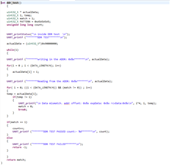
Hi,
Already we have tested SD card with ti/board/diag/mmcsd and it got passed.
nice, then we can concentrate on DDR.
We are doing same thing as you said by adding print message and checking where exactly it getting failed.
yeah, please let me know the updates.
Attached our own Mem test same as ti provided mem test code result and code snap which we have tested through JTAG interface
Can you run our mem test as that will give more clear picture about the start address and end adress of DDR. In your code, you are starting from 0x90000000 but ending is not clearly mention. Also DATA_LENGTH value is missing. Can you run the mem test..... we have macro for start and end address....just update that according to your custom board, build and run.
Also, are you updating the DDR start and end address in the board_library/board_cfg.h file. Because, sbl will pick up from that file only.
Hi Anubhav,
thanks a lot. SD card boot up is working with our new MLO. please find our changes in board_library files.
> WE updating the DDR start and end address in the board_library/board_cfg.h file as per our custom board DDR size.
> "ti\board\src\idkAM572x\idkAM572x_ddr.c" -> we added GEL file output to idkAM572x_ddr.c that we generated from DDR emif tool. and also added emif tool generated dmm_lisa_map_regs in register values(U-BOOT) into AM572x_set_lisa_maps() function in idkAM572x_ddr.c file.
Regards,
Rajeshwar