


Part Number: 66AK2G12
Hi I am designing my board with the Ti SOC 66ak2g12
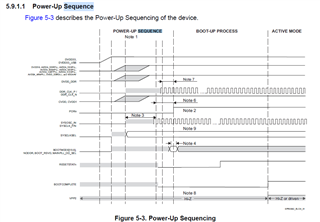
The datasheet states that the SOC power up sequence is as this order (using figure 5-3) :
3.3V (DVDD33) then 1.8V,1.0V DDR and Core voltage.
The Artix family of FPGA by Xilinx requires the opposite sequence first FPGA core1.0V, then 1.8V_AUX and lastly the 3.3V I/O.
- I see two options that can be to power on the SOC+ FPGA :
- 0VFPGAcore ->1.8V FPGA_Aux -> 3.3VFPGA and_SOC_IO -> 1.8VDDR+1.0VSOC_core
- 3V_SOC_IO(only) -> 1.8VDDRand FPGA_AUX+1.0V_SOC_core ->3.3V FPGA_IO(only)
Both option have possibility of leakage voltage that will cause the power up to be from certain voltage and not from 0V. (for example the in B, before turning on the FPGA 3.3V IO the FPGA will have ~~2.3V.
Similarly in option a I fear that the SOC might have leakage voltage on the 1.8V and core voltage before turning them on. (That leakage will come from the FPGA IOs connected to SOC)
Please advise at what order do you recommend to perform the power up/ down sequence ? and your comments on the above.
- Do you have application note or evaluation board combining the two SOC (Keystone2 and Artix FPGA ) ?
- Please take a look at Ti’s article on power sequence :
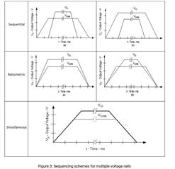
At what type of implementation the SOC power should be ? sequential , radiometric or simultaneous ?
- If I use simple voltage monitor that causes reset when power is down. Meaning the requirement of resetting the SOC before the power is down, is kept, what is the importance of the power down ? meaning if the power down sequence is not kept what will happen. Remember that the power down period is of few milliseconds.
Thanks
Avner
