This thread has been locked.

If you have a related question, please click the "Ask a related question" button in the top right corner. The newly created question will be automatically linked to this question.

AM3352: Jitter peak-to-peak, LVCMOS reference clock period specification

Part Number: AM3352

Hi Team,


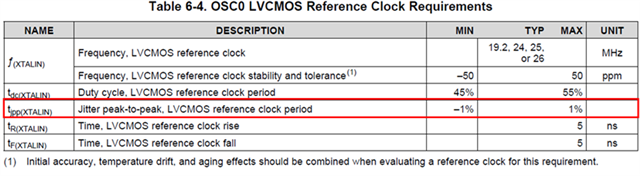
Jitter peak-to-peak is defined in the data sheet by the red border as below.

My customer would like to have a graphic representation of the TI-defined Jitter peak-to-peak.

Do you have any document for it?

Would you please explain What is TI-definition for this parameter?

How to calculate it?


Would you also tell me what the impact might be if tjpp(XTALIN) cannot be satisfied?


Thanks and Best regards,

Kuerbis

  • The jitter parameter defines peak-to-peak period jitter, which effectively defines the worst case minimum clock period and worst case maximum clock period relative to the average clock period. The min limit of -1% is saying the clock period should never be less than 99% of its average period and the max limit of 1% is saying the clock period should never be more than than 101% of its average period. For example, the worst case minimum clock period should be 39.6 ns and the worst case maximum clock period should be 40.4 ns when using a 25 MHz reference clock average clock period with a 40.0 ns average clock period.

    The clock stability and tolerance parameter defines limits associated with the average clock frequency, which can be used to determine the average clock period. The average clock frequency can vary by +/-50 ppm, or +/- [0.00005 x (reference clock frequency)]. For example, the average clock frequency can range from 24.99875 MHz to 25.00125 MHz when using a 25 MHz reference clock. This means the average clock period can vary from 39.998 ns to 40.002 ns.

    Hopefully, the above descriptions will help answer your customer’s questions. If not, they should be able to google period jitter and find additional information on this topic.

    Regards,
    Paul