This thread has been locked.

If you have a related question, please click the "Ask a related question" button in the top right corner. The newly created question will be automatically linked to this question.

AM5726: Spread Spectrum Clocking Configuration

Guru 10285 points

Part Number: AM5726

Hi Support Team,

My customer is starting to experiment with SSC.

DRA7xx, AM57xx, TDA2x, TDA3x Spread Spectrum Clocking Configuration App Report
https://www.ti.com/lit/an/spraby0a/spraby0a.pdf

2.2.4 Example Application

My customer is attempting to configure a prototype using the examples in this document,
and would appreciate answers to the following questions.


Q1. In this example, the EMI countermeasure is for a 50MHz application, but in this application,
  the dot clock (pixel clock) of the LCD is assumed to be 33MHz.
  In this case, is it correct to understand 50MHz as 33MHz?

Q2. I need the frequency of CLKINP. Is it correct to understand that it is CLKINP of DPLL_VIDEOx
  as described in Figure 11-10. VIDEO PLL Reference Diagram of TRM?

Q3.  In the PLLCTRL_VIDEOx block above, HIGHFREQ: 0=divided_by_2, 1=not_divided is described.
  However, TRM: In the PLL_CONFIGURATION2 register description

root@am57xx-evm:~# devmem2 0x58004310 /*PLL_COMFIGURATION2
[12] PLL_HIGHFREQ
0x0: Pixel clock is not divided
0x1: Pixel clock is divided by 2
This is described as follows.

  If this is the correct description, please explain the difference.
  Also, if this difference is not correct, please provide the correct information.

Q4.  I need the values of N, M, and M4.
  Is it correct to understand that the references and values are as follows?
  The following values are read from the prototype, but the current settings are equivalent to EVM,
  so I believe the values are the same.

   root@am57xx-evm:~# devmem2 0x5800430c /*PLL_COMFIGURATION1
   /dev/mem opened.
  Memory mapped at address 0xb6f8a000.
  Read at address 0x5800430C (0xb6f8a30c): 0x010DEC4E /*value

[25:21]=01000 ∴ M4= 8
[20:9]=011011110110 ∴ M= 1782
[8:1]=00100111 ∴ N= 39

Best regards,
Kanae

  • Kanae,

    Q1 -- Please see Figure 1 of App Note: 50MHz is nominal frequency; 33 KHz is the modulation frequency (which creates the triangular modulation)

    Q2 -- CLKINP is the input clock; your understanding is correct note that if CLKSEL is 0, CLKINP is VIDEOx_DPLL_CLK

    Q3 -- bit 12 does control the HIGHFREQ mux

    Q4 -- I agree with your decode of PLL_CONFIGURATION1 -- If you had a 20MHz CLKINP, these values would lead to 99MHz output clock [20 [MHz]/(39 + 1) * 1782 /(8 + 1) =99 [MHz]

    Kevin

  • Hi Kevin,

    Thank you for your reply.
    I will share your contact information with my customer.

    Please allow me to confirm your answer to Q3.

    >Q3 -- Bit 12 controls the HIGHFREQ mux.

    Does this mean that the following statement
    in the PLL_CONFIGURATION2 register of TRM is correct?

    /*PLL_COMFIGURATION2
    [12] PLL_HIGHFREQ
    0x0: Pixel clock is not divided
    0x1: Pixel clock is divided by 2
    This is described as follows.

    Is HIGHFREQ: 0=divided_by_2, 1=not_divided
    described in Figure 11-10 above a misprint?

    Best regards,
    Kanae


  • Hi Kevin,

    Here is an additional question.

    Q5. My customer is considering setting the following two conditions.

    1. The conditions that have the greatest impact on the system in the configurable range.
       Modulation_depth 3.00%
       Modulation_rate 100kHz

    2. The conditions that have the least impact on the system in the settable range.
       Modulation_depth 0.50%
       Modulation_rate 30kHz

    *Both 1 and 2 are center spread.

    I am currently looking at the reference example,
    but since I still don't understand the example,
    could you please tell me the parameter values to set the above condition?

    Here are my customer checked items.*******************************************************

    I still do not understand the parameters to set the above two conditions.

    root@am57xx-evm:~# devmem2 0x5800431c /*PLL_SSC_COMFIGURATION2

    [29:20]=>[29:23]= mantissa: I saw a change in modulation depth with this value change.
                   [22:20]= Exponential I saw a change in modulation depth with this value change.

    [19:0]=>[19:18]=Integer: I could not see any change in this value after changing it.
                 [17:0]=minority: I could not see any change in this value after changing it.


    The following are the specific values that I checked for frequency spread.

    Initial value: 0x58004318 = 0x00000000 0x5800431c = 0x00000000 No spreading

    Check 1:       0x58004318 = 0x00000001 0x5800431c = 0x0c040000 spread of about ±1.5%
    Check 2:       0x58004318 = 0x00000001 0x5800431c = 0x0c080000 spread of about ±2.9%,
    Check 3 (A): 0x58004318 = 0x00000001 0x5800431c = 0x0c0a0000 spread of about ±3.5%,
    Check 4:       0x58004318 = 0x00000001 0x5800431c = 0x0c0C0000 spread of about ±4.1%,
    Check 5:       0x58004318 = 0x00000001 0x5800431c = 0x05040000 spread of about ±0.5%,
    Check 6:        0x58004318 = 0x00000001 0x5800431c = 0x07040000 spread of about ±0.7%,
    Check 7 (B): 0x58004318 = 0x00000001 0x5800431c = 0x1f040000 spread of about ±3.6%,
    Check 8:       0x58004318 = 0x00000001 0x5800431c = 0x2f040000 spread of about ±5.5%,

    *All setting are Center spread and all check's modulation frequency are unknown.

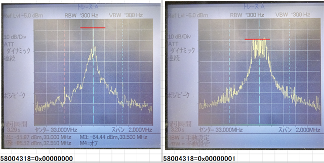
    As shown below, the degree of spread is almost the same for A and B,
    but the levels appear to be different.
    Can we consider this as a difference in modulation frequency?


    Spread spectrum image of A


    Spread spectrum image of B


    In the above case, is it correct to assume that
    the modulation frequency of B is higher than that of A?

    Best regards,
    Kanae

  • Please also send register for 0x5800_4310 (PLL_CONFIGURATION2)  Figures 11-10 and 11-17 conflict on the def of HIGHFREQ, but I want to know if it is pertinent. How is CLKSEL set?

    Q5 -- following the APP Note, I find that the settings violate  #3 -- that 30KHz or 100KHz is NOT LESS than REFCLK/70. Noting that 30KHz * 70 is 2.1MHz, the REFCLK would have to be at least that big. My guess is that the input clock frequency is around 20MHz, and REFCLK is then ~20MHz/(N + 1) = ~20MHz /(39 + 1) = ~0.5MHz. In order to use the spreading, you will need to re-configure the N and M dividers.

    If you respond further to this message, please include the input clock rate.

    Kevin

  • Figures 11-10 and 11-17 differ on this polarity. Please send PLL_CONFIGURATION2 value as CLKSEL = 0 makes this bit moot.

    Kevin

  • Hi Kevin,

    Thank you for your reply.

    Regarding Q3, I have asked my customer to share the register value, so please wait.
    However, please tell me how to understand this inconsistency in the case of CLKSEL = 1.

    As for Q5, I will share the information with my customer.
    I think the input clock is 20MHz, but I will specify the confirmed value
    when I ask additional questions.

    Best regards,
    Kanae

  • Hi Kevin

    I have the following comments from my customer for each your answer and confirmation.

    Q1--
    Kevin> Please see Figure 1 of App Note: 50MHz is nominal frequency; 33 KHz is the modulation frequency (which creates the triangular modulation)

    For this application, the dot clock of the LCD is assumed to be 33MHz.
    The modulation frequency is assumed to be 33 kHz.
    In this case, is it correct to understand that the nominal frequency is 33MHz?

    Q3--
    Kevin> Please send PLL_CONFIGURATION2 value as CLKSEL = 0 makes this bit moot.

    The register value of 0x5800_4310 (PLL_CONFIGURATION2) is as follows.

    root@am57xx-evm:~# devmem2 0x58004310
    /dev/mem opened.
    Memory mapped at address 0xb6f22000.
    Read at address 0x58004310 (0xb6f22310): 0x00616008

    Therefore, we assume that 20MHz is input to DPLL_VIDEOx_CLKINP.


    M7 and M6 clocks are set to disabled.
    M4 clock is set to enable.
    Since CLKSEL = 0, VIDEOx_DPLL_CLK is supplied to DPLL_VIDEOx.

    From TRM Figure 3-43, SYS_CLK1 (OSC0) is selected for VIDEO1_DPLL_CLK,
    and its frequency is 20MHz.


    Q4--
    Kevin> [20 [MHz]/(39 + 1) * 1782 /(8 + 1) =99 [MHz]].

    Isn't the "99MHz" calculated here output directly to vout1_lk?
    The output frequency of vout1_clk is 33MHz, so I think it is 1/3 of the output frequency.
    I'm still investigating where the 1/3 multiplier is, but I'm stuck in this investigation
    and haven't been able to go any further.

    Q5--
    Kevin > I find that the settings violate  #3 -- that 30KHz or 100KHz is NOT LESS than REFCLK/70. 

    Thank you for your reply. I have confirmed the current situation as follows.

    REFCLK=CLKINP/(N+1), CLKINP=20MHz fixed

    N= 39MHz REFCLK= 0.5MHz
    REFLK/70=7.142857143kHz Modulation frequency 33kHz
    *Judge the value of N: WRONG>>> Current status is violated.

    N= 7MHz REFCLK= 2.5MHz
    REFLK/70=35.71428571kHz Modulation frequency 33kHz
    *Judge the value of N: CORRECT>> If N=7 or less, it seems to be able to comply, so we will reselect within this range.

    N= 1MHz REFCLK= 10MHz
    REFLK/70=142.8571429kHz Modulation frequency 100kHz
    *Judge the value of N: CORRECT>> If we raise the modulation frequency to the upper limit, it seems that only N=1 will be selected for the current CLKINP.

    I look forward to your answers to the additional questions above,
    as well as your comments and advice on customer recognition.

    Best regards,
    Kanae

  • Q1 -- You are generating 99MHz from the PLL; I think there are dividers later which (if set to divide by 3) would cleanly get you to 33MHz. From the pixel clock perspective, 33MHz is the nominal frequency.

    Q3 -- CLKSEL selects SYSCLK (as you write); HIGFREQ is moot.

    Q4 -- the are LCD and PCD dividers that create the pixel clock; in my TRM version, this is listed under DISPC Clock Configuration

    Q5 -- you are right; changing the N value will increase the REFCLK, making 33KHz and / or 100KHz modulation feasible. You have identified that you need a minimum REFCLK equal to 2.31MHz in order to hit 33KHz modulation and a minimum REFCLK equal to 7MHz in order to support 100KHz modulation.

  • Hi Kevin,

    Thank you for your support!
    I have shared your reply with my customer,

    Here is an additional question.

    Q6. 
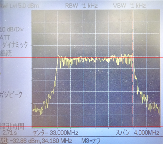
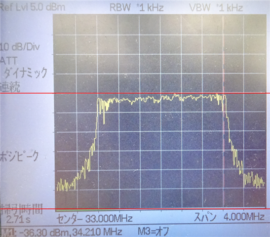
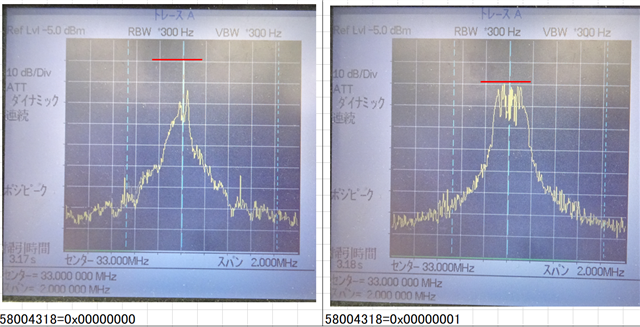
    Regarding the relationship between the PLLCTRL_VIDEOx setting and the signal waveform,
    is there a mistake in the setting that causes the modulation level (intended to be 3%) to occur
    only about 1%, although the peak level drops about 10 dB?

    The data is as follows. 

    Best regards,
    Kanae


  • Hi Kevin,

    I have received the following additional questions from my customer
    who have further verified, and would appreciate your views.

    Q7.
    Regarding the relationship between the setting of PLLCTRL_VIDEOx
    and the signal waveform, when I changed the clock to CLKINP of DPLL_VIDEO1
    as shown below under the condition of no modulation,
    jitter was generated in the clock of vout1.

    What are the conditions/reasons why this jitter may occur?

    Before the change
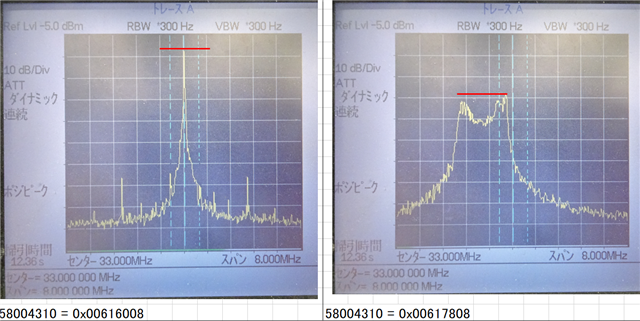
    58004310 = 0x00616008 

    After change
    58004310 = 0x00617808

    Register setting;


    Waveform;

    Q8.
    Also, when I changed the register settings as shown below, no change occurred.
    For (1), I think it is the correct result because CLKSEL=0, so HIGHFREQ is not affected,
    but for (2), is it the correct result that no change occurs?

    (1) 58004310 = 0x00617008
    HIGHFREQ=1(divided by 2), CLKSEL=0(PCLK)


    (2) 58004310 = 0x00616808
    HIGHFREQ=0(not divided), CLKSEL=1(SYSCLK)

    Best regards,
    Kanae

  • Kanae

    In response to Q6, try increasing REFCLK frequency a little more and see if the spread starts to be clearer. (I am not sure that this is the correct idea, but it is my best idea.)

    Q7 -- this result does not surprise me; the higher jitter clock is sent through a circuit that is intended to divide the clock (although in this case, you have chosen not to divide). It seems likely to me that the extra circuitry could add jitter.

    Q8 -- when CLKSEL is 0 (0x617008), it chooses SYSCLK and HIGHFREQ and REFSEL are don't care;

    when CLKSEL becomes 1(0x616808), the HIGHFREQ divider does affect the output frequency; here HIGHFREQ is 0 which according the bit description means that the clock is NOT divided. That interpretation of the clock path makes sense when you report than no change occurred.

    Kevin

  • Hi Kevin,

    Thank you for your support.

    Here is the results that my customers have tried.

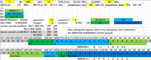
    Q6 - For example, I made the following changes,
    and DSS_CLK (monitor vout1_clk) remained unchanged at 33MHz,
    and the degree of spreading was almost unchanged.

    The peak level drops by about 10dB, but the modulation (intended to be 3%)
    seems to occur only about 1% of the time.


    Could you please reply how else I can check the conditions
    under which this status has occurred?

    Best regards,
    Kanae

  • Kanae,

    I do not understand the pictures. The new frequency is at 44.4MHz but what you show seems to be at 33MHz.

    Kevin

  • Hi Kevin,

    Thank you for reply.
    My customer is also concerned about this you pointed.

    If he try to increase the frequency of REFCLK,
    there is not any change in the spread starts as the above post.

    When you say "try to increase the frequency of REFCLK",
    do you mean that the clock frequency used looks the same,
    but the clock source is actually different?

    Best regards,
    Kanae

  • Kanae,

    I do not think your customer measured the clock correctly. If you look at the pictures uploaded, I believe that both are measuring the emissions at a central frequency of 33MHz.; however, when your customer increased the REFCLK frequency (as requested), he calculates the DSS_CLK at 44MHz. So, I'm not sure what a measurement at 33MHz tells me...

    Kevin