This thread has been locked.

If you have a related question, please click the "Ask a related question" button in the top right corner. The newly created question will be automatically linked to this question.

AM6548: Boot mode pins state during device reset

Part Number: AM6548
Other Parts Discussed in Thread: TPS54618, TPS62827,

Hi all,

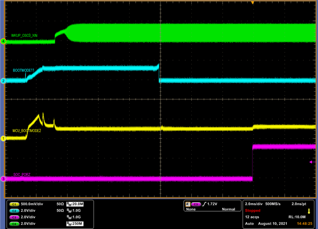
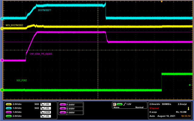
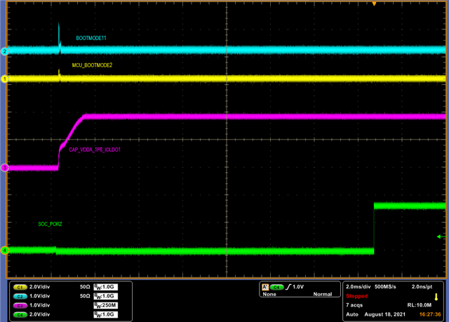
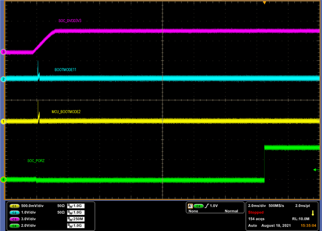
During the HW verification process of our board with the X6580AACD device, we have noticed a strange behavior of BOOTMODE and MCU_BOOTMODE pins.  The screen snapshot of measurement is presented below:

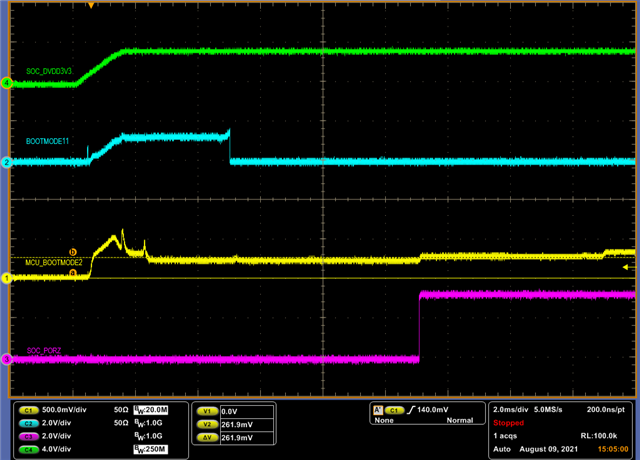
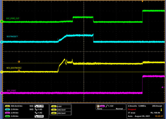
MCU_BOOTMODE2 and BOOTMODE11 are selected since they are pulled down with resistors of 100K (the same resistors were used in our previous version of PCB with X6580ACD device and on IDK board as well). The screen snapshot of the same measurement with SOC_PORZ_OUT signal is presented below:

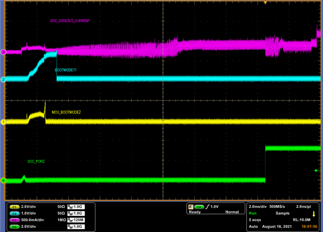
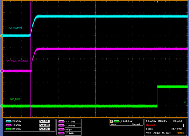
From previous snapshots, it can be seen that, for some reason, it seems that internal pull-up resistors on MCU_BOOTMODE pins remain active during the SOC_PORZ signal active state which is not expected according to the datasheet. 

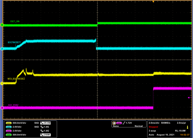
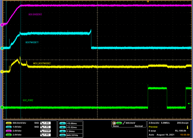
As Sitara SoC starts to heat up the voltage level on the MCU_BOOTMODE pins starts to rise to reach more than 500mV.

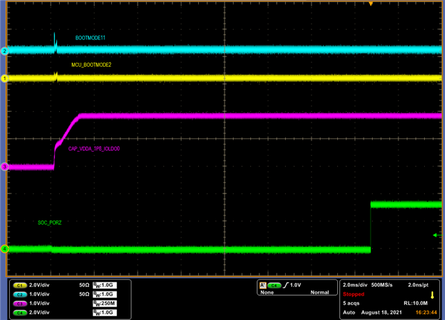
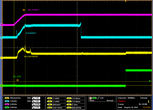
At some point, after additional heating, the MCU_BOOTMODE pins, as well as BOOTMODE pins start to behave normally:

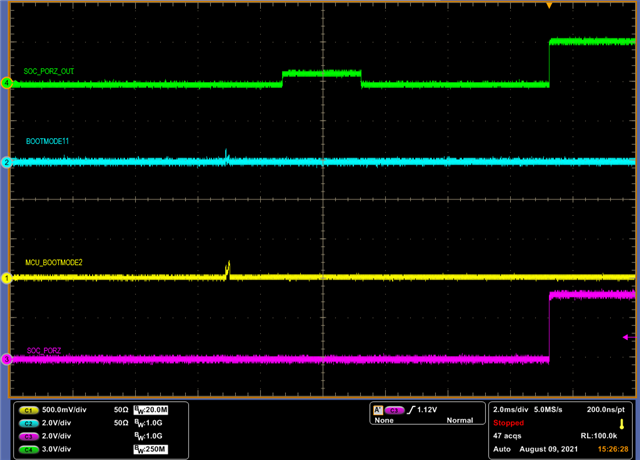
As a result, on some boards, the wrong boot mode was selected. For example, since MCU_BOOTMODE2 is responsible for selecting reference clock logic 1 is selected instead of logic 0 (No PLL Configuration Done (slow speed backup) instead of 25MHz reference clock).

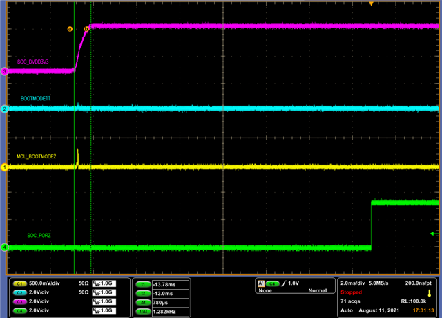
In our reset configuration, MCU_PORZ and PORZ pins are connected together, the MCU_BYP_POR signal is pulled high and PORZ_OUT and MCU_PORZ_OUT are pulled low by two resistors. 

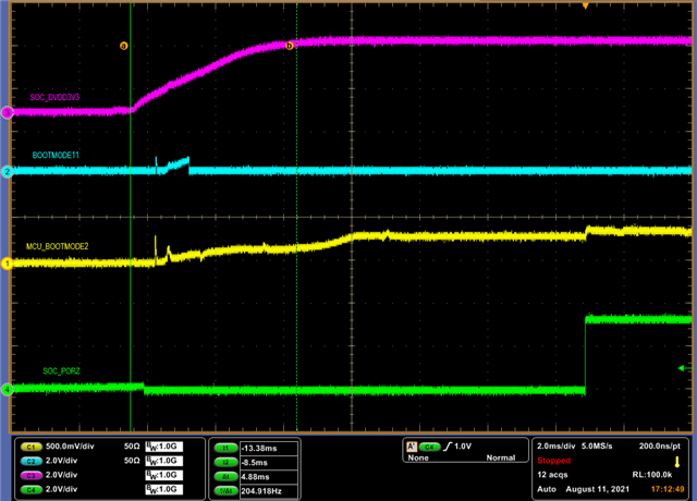
Just to mention, on the previous version of our board with the X6580ACD device and identical reset configuration the BOOTMODE and MCU_BOOTMODE pins are behaving properly.

My question is what can be done to prevent this Boot mode pins behavior? Also, is there some explanation for what we are measuring?

Best regards,

Zoran Dukic

  • Hello Zoran,

    Can you probe the OSC1 and WKUP_OSC0 inputs at the same time?  

    Thanks,

    Kyle

  • Hi Kyle,

    Thanks for the reply,

    Screenshots are below:

    In our case OSC1 is not used, so the OSC1_XO pin is left floating, and OSC1_XI pin is tied to the ground using a 10K resistor.

    Regards,

    Zoran

  • Zoran,

    OK, your connections make sense as the data manual clearly shows OSC1 as optional.

    As a debug experiment, can you connect a clock to OSC1 to see if that changes the behavior?  You can connect a function generator with 1.8V signaling as summarized in the data manual diagram titled "1.8-V LVCMOS-Compatible Clock Input"

    Thanks,

    Kyle

  • Kyle,

    I've connected the function generator as requested. However, behavior remains the same.

    Regards,

    Zoran

  • Can you capture the power rails for these IO banks (waveforms above)?  For example - when SOC_PORz_OUT IO is mis-behaving, can you also capture VDDSHV0 (IO rails for SOC_PORz_OUT).  Similarly for BOOTMODE pins?  Have you confirmed the power sequence documented in the data manual is being followed?  If rails are energized in the incorrect order - could cause unknown behavior of the device (from leakage/latchup within the device).  Any other circuitry connected to these signals (SOC_PORz_OUT, BOOTMODE, etc)?

  • Hi Robert,

    Thanks for the reply. I've checked the IO banks power supply rails and I'm sure that we don't have any issues there. If you look at the first screenshot I've provided, you will see that issues start to appear while 3V3 rail is still rising. So, at that moment, there are no other power supply rails active.

    Our previous PCB version which works correctly is using different DC/DC converters (TPS54618). There, 1ms soft start-up time is selected. In the new PCB version, the DC/DC converter used is TPS62827 where the soft start-up time is typically 1.75ms (according to the datasheet).  So I've tried to play a little bit with the SOC_DVDD3V3 slew rate. For this purpose, I've connected the output of TPS54618 DC/DC converter from the old board (since this device supports start-up time adjustment) to 3V3 power supply rail on the new board. Of course, some adjustments were necessary to provide proper power supply sequencing. 

    Here are the results for 800us SOC_DVDD3V3 rise time:

    So, with fast SOC_DVDD3V3 Sitara BOOTMODE and MCU_BOOTMODE pins behaves properly. 

    Now, I've changed the SOC_DVDD3V3 start-up time to almost 5ms. The screenshots are presented below:

    So, the strange behavior of BOOTMODE and MCU_BOOTMODE pins is back again.

    I don't have the possibility to play with different values of SOC_DVDD3V3 start-up time (since our stock of 0201 X7R capacitors is very limited). For sure, 1.75 ms start-up time is not good enough and 0.8ms is working. 

    My question would is it possible that SOC_DVDD3V3 slope can trigger this BOOTMODE and MCU_BOOTMODE pins behavior? In the datasheet for AM6548 only the maximum power supply slew rate is specified. Is there a limitation regarding minimum slew rate values?

    Regards,

    Zoran 

  • Is there anything else connected to the BOOTMODE pins - or simply external PU/PD resistors?

    For the IO banks that are 3.3V - what are the associated VDDS supplies sourced from?  For example, BOOTMODE11 is on pin P27, which is IO bank VDDSHV2.  What supply is used to power VDDS2?

  • Hi Robert,

    There is nothing on BOOTMODE  pins except pull-up or pull-down resistors. The same applies to all MCU_BOOTMODE pins except for MCU_BOOTMODE5, MCU_BOOTMODE6  and MCU_BOOTMODE7 which are connected to the NVRAM SPI interface. This NVRAM device /CS is pulled up to the same power supply rail which powers the VDDSHV0_WKUP.

    VDDSHV2 (BOOTMODE pins) and VDDSHV0_WKUP (MCU_BOOTMODE pins) are connected to the same DC/DC converter output (which generates SOC_DVDD3V3 power supply rail mentioned above).

  • Sorry if I wasn't clean in my question.  I understand the supply power for VDDSHV2, but what about VDDS2?  This is the BIAS supply for the IOs when using 3.3V.  It should be connected (powered from) CAP_VDDA_1P8_IOLDO0.  This CAP_* pin in an internal LDO output, which is source from input VDDA_3P3_IOLDO0 (should be supplied by same 3.3V as VDDSHV2).  Can you confirm?  

  • I confirm that. 

  • Robert,

    Bumping this up - this was raised as priority during an offline conversation with the customer.

    Regards

    Karthik

  • Hello Zoran,

    The glitch on IO output during supply ramp up is expected when the supply is NOT stable. But it should go away as soon as the supply is stable.

    But stuck at non HiZ state even after the supply is stable is not expected behavior.

    Can you share the following additional information: 

    1. Is it repeatable across multiple parts or occurs only in few samples?
    2. Please share VDDS/CAP_VDDS_1P8V_IOLDO* waveforms. Also the current through 3.3v supply/VDDSHV, if available.
    3. What is the behavior with Temperature. Does it get better or worse with increasing temperature? Consider two types of scenarios.
      1. Set the temperature to desirable value. and go through boot sequence. Observe the no of pins and the final voltage level on failing pins.
      2. Boot up at room temp and once supply is stable, increase/decrease the temp and observe for the correct pin functionality.   
    4. Does it go away if soc_porz is toggled? i.e. 0-1-0-1 instead of 0-1.

    Thanks,

    Kyle

  • Hello Kyle,

    1. Yes, this is repeatable across multiple parts.

    2. If you are referring to VDDS_1P8V_IOLDOx voltages those are connected to the 3.3V DC/DC converter output. CAP_VDDS_1P8V_IOLDO0 waveform for the cold board is presented below:

    CAP_VDDS_1P8V_IOLDO0 waveform for the hot board (hot means that Sitara junction temperature is above 60 ̊ C) is presented below:

    As the junction temperature rises, the part of CAP_VDDA_1P8V_IOLDO0 where we have an overvoltage becomes shorter and shorter until it disappears completely. 

    CAP_VDDS_1P8V_IOLDO1 waveform is presented below:

    Here we don't see any dependency on temperature.

    Current through the 3V3 power supply is presented below:

    Here we don't see any dependency on temperature, also. 

    3. It gets better as the temperature rises. The threshold is somewhere at 60-65 ̊C junction.

    Screenshot of BOOTMODE11, MCU_BOOTMODE2, SOC_PORZ and 3V3 power supply rails for cold (room temperature) is presented below:

    The same diagram when the board is heated (junction temperature around 40 ̊C is presented below:

    It can be seen that the width of BOOTMODE11 where it is irregular becomes shorter as the temperature rises. Also, the voltage level of MCU_BOOTMODE2 rises with the increase of temperature.  

    The same diagram when the junction temperature rises over 60-65 ̊C is presented below:

    All diagrams were made with the 3V3 power supply rise time of 1.5ms. When we use the test setup with the 3.3V power supply rail rise time below 1ms, the strange behavior disappears completely.

    Snapshot with 1.5ms 3V3 rise time:

    Snapshot with 0.8ms 3V3 rise time (the same test conditions, same board, same temperature):

    I will provide the snapshot with 0101 SOC_PORZ toggling in a separate post.

    Regards,

    Zoran

  • Diagrams with 0101 SOZ_PORZ toggling are presented below:

    So, the SOC_PORZ toggling doesn't help.

    Regards,

    Zoran

  • Hello Zoran, 

    Thanks for the additional info.  We are reviewing this with our design team.

    What are your thoughts on how to resolve the issue.  Is there a convenient way for you to implement a faster ramp time on the 3.3V domain?

    Thanks,

    Kyle

  • Hello Kyle,

    Right now we don’t have any solution to increase the slew rate at the 5V/3V3 DC/DC converter output. The fact is that we are using the DC/DC converters which are proposed by TI and which don’t have any possibility to control the slew rate.

    Now, we are trying to find out a solution that wouldn’t require PCB redesign and with this in mind we are focused on very simple solutions with the minimum component count. The fact is that we are trying to effectively bypass the DC/DC converter during the start-up phase. Also, the bypass circuit should be switched off once the 5V/3V3 DC/DC converter is started. We’ve tried with forward diodes (two or three of them connected in series) but forward voltage is highly dependent on temperature meaning that what seems to be working at room temperature will probably not work at 95C which is the maximum ambient temperature in our use case. Also, the Zener diode didn’t help. The last thing we would try is to use an additional 3V3 LDO connected in parallel with 5V/3V3 DC/DC converter. The output of LDO will be connected through the Schottky diode. Hopefully, this way we will be able to create a fast slope at the 3V3 power supply rail.

    Do you have any news on this topic? We don’t know is there something that is going on your side in the background? I suppose that you have a post-silicon validation/characterization platform for Sitara processor. Are you able to recreate this boot-mode pins behavior with a slow ramp at the 3V3 power supply rail on your side?

    Best regards,

    Zoran

  • Zoran,

    We have managed to reproduce this issue on our EVM.  We are working with our design team to understand root cause and potential recommendations.

    Regards,

    Kyle

  • Zoran,

    We have identified that changing the load capacitor on CAP_VDDA_1P8_IOLDO0  from 2.2uF to 3.3 uF resolved the issue for our EVM.

    Can you try this to see if it improves the situation on your side?

    Thanks,

    Kyle

  • Hello Zoran,

    I am in the process of reviewing the provided test report (provided via TI box, not on this thread)  with our internal experts.

    We have the following questions/comments:

    - Is it possible that there is some SoC IO that is driven or pulled high before the SoC 3.3V vddshv supply ramps up?  (We are double checking your schematic for the same, would be good for you to check as well)

    - Or is any supply to the SoC ramping before the 3.3V vddshv supply ramps up?

    - In addition to the evaluation criteria for BOOTMODE11 and MCU_BOOTMODE2 .... can you probe the CAP_VDDA_1P8_IOLDO0 on one or more of the systems with the "LDO + Diode workaround" implemented?  Does it stabilize at 1.8V or does it have a momentary excursion above 1.8V?  What is the magnitude and duration of that excursion?

    - TI does not have any concerns with your proposed workaround (LDO+diode).  Your scope traces show that the vddshv 3.3V signal ramps monotonically and stays within the specified recommended operating conditions.

    Regards,

    Kyle

  • Hello Kyle,

    Bellow is the scope snapshot of the 3V3 power supply and CAP_VDDA_1P8_IOLDO0 with LDO + diode workaround implemented. 

    Btw, I've already provided scope snapshots of CAP_VDDA_1P8_IOLDO0 (on August the 19th) for two slew rate values of 3V3 power supply rail (fast and slow ramp). With a slow ramp on 3V3 we've observed the excursion above 1V8 - to around 2.8V for a period of around 7ms.

    Regards,

    Zoran

  • Hello Zoran,

    I sent an email with the following but I don't think received a response.  Posting here as a follow-up:

    Is the “stronger pull on bootmode” able to resolve the issue independent of the supply ramp rate? 

     What is your status/proposal on the “ramp rate” speed-up?  Is it to use a different PMIC/Buck to drive the rail?  Or is it still to use the diode+LDO circuit?

     Re: your questions:

     -1-

    Root cause?

     We are attempting to reproduce the issue on ATE (production tester) since that platform could isolate the different supplies and IOs.  So far we have been unsuccessful at seeing the same issue there.  We are trading parts between ATE and Bench to attempt to correlate the observations on the two platforms.

     -2-

    Are other parts of SoC impacted by the 3V3 power?

     I would expect the impact to only be on the 3.3V IOs (that is the only domain that the 3V3 power is feeding).  Other pins with weak pulldowns could potentially see the same type of behavior.  If that’s the case it may be less likely for there to be an obvious issue compared to the BOOTMODE pins which clearly need to be at the desired level when they are latched during the power up and reset sequence.

    Regards,

    Kyle