This thread has been locked.

If you have a related question, please click the "Ask a related question" button in the top right corner. The newly created question will be automatically linked to this question.

TDA2PXEVM: AUXCLK value calculation

Part Number: TDA2PXEVM


Hi TI Team,

I have a question related to how to calculate the AUXCLK value for TDA2PXEVM McASP module.

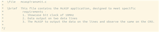
I am trying to use the McASP transmit example provided in the CSL folder in the pdk:

~/PROCESSOR_SDK_VISION_03_08_00_00/ti_components/drivers/pdk_01_10_04_05/packages/ti/csl/example/mcasp/mcasp_transmit

I reviewed the TDA2Px Technical Reference Manual, and the following steps I used to figure out how to calculate the AUXCLK.

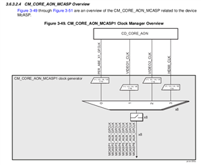
1. from "3.6.3.2.4 CM_CORE_AON_MCASP Overview", I can see the different possible sources of the McASP3_AUX_GFCLK and by reading the "CM_L4PER2_MCASP3_CLKCTRL[23:22] CLKSEL_AUX_CLK" (value 0) register, I can confirm that the "PER_ABE_X1_GFCLK" source is used.

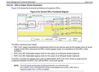
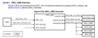
2. from "3.6.3.6.1 DPLL_ABE Overview", I can see that the "PER_ABE_X1_GFCLK" signal source is "ABE_DPLL_CLK" signal after passing the "DPLL_ABE" module.

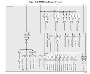
3. from "Figure 3-40. PRM Clock Manager Overview", I can see the different possible sources of the "ABE_DPLL_CLK" and by reading the "CM_CLKSEL_ABE_PLL_REF[0] CLKSEL" (value 0) and "CM_CLKSEL_ABE_PLL_SYS[0] CLKSEL" (value 1) register, I can confirm that the "SYS_CLK2" source is used.

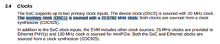
4. from "TDA2Px-ACD CPU EVM Board User's Guide" section "3.4 Clocks", The auxiliary clock (OSC1) is sourced with a 22.5792 MHz clock.

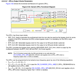
5. back to the "DPLL_ABE module", section "3.6.3.3.2 DPLLs Output Clocks Parameters" describes the calcution of the "PER_ABE_X1_GFCLK" output signal from "ABE_DPLL_CLK" input signal.

This depends on the M, N and M2 values besides the CM_CLKMODE_DPLL_ABE[11] DPLL_REGM4XEN.

these values are as follows:

M "CM_CLKSEL_DPLL_ABE[18:8] DPLL_MULT", is 200

N "CM_CLKSEL_DPLL_ABE[6:0] DPLL_DIV", is 9

CM_CLKMODE_DPLL_ABE[11] DPLL_REGM4XEN, is 0

M2 "CM_DIV_M2_DPLL_ABE[4:0] DIVHS", is 1

So, if I applied all the above sources, I can get that the AUXCLK equals to 451.584 MHz.

back to the "mcasp_transmit" example, it claims that the bit clock should be 10MHz by using "CLKXDIV" value 2 which results in value 3 and "HCLKXDIV" value 5 which results in value 6.

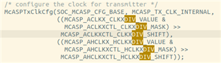
if the AUXCLK equals 451.584 MHz, and CLKXDIV" value 2 and "HCLKXDIV" value 5 , the bit clock should be 25.088 MHz not 10MHz as claimed

I need your help to figure out why my calculations does not match the claimed value as I will depend on these calculations for my application.

your input is highly appreciated.

Best regards,

Ahmed

  • Hi,

    As you have already mapped clock lines for MCASP3, i suggest verify your theory through CLOCK TREE TOOL available at https://www.ti.com/tool/CLOCKTREETOOL. This will give you registers wise details also in the trace section. 

    Also have you probed and see what is the actual bit clock coming?

  • Hi Anubhav,

    Thanks you so much for your feedback, the tool really helped me a lot and corrected the value that I previously calculated.

    The AUXCLK value should be 903.168 MHz not 451.584 MHz unlike I mentioned before.

    Still this value can't give me the 10 MHz bit rate mentioned in the mcasp_transmit example.

    I did not measure the actual bit clock but I am planning to do this soon.

    I will update you with the value as soon as I get it.

    Thanks and regards,

    Ahmed

  • Hi,

    Still this value can't give me the 10 MHz bit rate mentioned in the mcasp_transmit example.

    Please try probing it. It may be a typo in the code.

    Using Clock tree tool you can do your calculations(permutations and combinations of all clock divider) to get the final bit clock frequency.

    I will update you with the value as soon as I get it.

    sure.

  • Hi Abubhav,

    I almost can calculate the clock and match the measured ones.

    I have an issue with a note stated in this section:

    it is all about the divider by 2 after the M2 divider, firstly I was taking it into my calculation and concluded that the AUXCLK should be 451.584 MHz but when I used the CTT tool I found that the value of the AUXXLK is 903.168 MHz.

    after getting back to the documentation, I found the previosly mentioned note and thought that this divide by 2 value after the M2 divider is not applied to DPLL_ABE module (only applied to MPU module under certain condition ) but the measured value confirmes that the AUXCLK must be 451.584 MHz not 903.168 MHz.

    So, is there any way from the resopsble team in TI to confirm whether I should consider this divide by 2 or not?

    if this divide by 2 should be considered, I think the CTT tool should be fixed to consider it as well.

    I have a very strong belief that the CTT is switching the "CLKOUTX2_M3" , "CLKOUTX2_M2" and "CLKOUT_M2" of the DPLL_ABE module.

    Please consider this figure:

    The "DPLL_ABE" module outputs should be from left to right in the previous figure "CLKOUT_M2" then "CLKOUTX2_M2", then "CLKOUTX2_M3" as the first pin from left is connected to "DPLL_ABE_CLKOUT_M2" and the second pin is connected to "DPLL_ABE_CLKOUTX2_M2" and the last one connected to "DPLL_ABE_CLKOUTX2_M3". 

    To confirm what I am thinking, I changed the M3 value in the DPLL_ABE module and I found that the second pin "DPLL_ABE_CLKOUTX2_M2" is the one that is changed while the last pin "DPLL_ABE_CLKOUTX2_M3" is the one whcih should change.

    by comparing the values stated in the DPLL_ABE module and what is shown on the clock tree block digram we can see the following:

    beside the "CLKOUT", the value is "451.5 MHz"

    beside the "CLKOUTX2", the value is "903.1 MHz"

    beside "M3", the value is "903.1 MHz"

    This were the expected values to be in the clock diagram but we can see that "CLKOUT" is wrongly connected to "CLKOUTX2_M3" and the "CLKOUTX2_M3" is wrongly connected to "CLKOUTX2_M2".

    it will be great if you can confirm my findings.


    Thanks and regards,

    Ahmed 

  • Ahmed,

    In general the TRM should be trusted compared to the CTT in this type of example.

    Regards,

    Kyle