This thread has been locked.

If you have a related question, please click the "Ask a related question" button in the top right corner. The newly created question will be automatically linked to this question.

TMS320C6747: EMIFA Parallel NOR Flash Interface

Part Number: TMS320C6747
Other Parts Discussed in Thread: TMS320C6745

Hello, 

I'm designing circuits with TMS320C6747.

My system requires a 64MB (512Mb) parallel NOR flash (Address[0:24]) for storing boot image.

I have a question about connecting external NOR flash memory to EMIFA interface.

According to spruh91d.pdf, TMS320C6745,C6747 DSP Technical Reference Manual the reference manual,

it is possible to interface with memory larger than 32KB by connecting the GPIO pins.

Also, as sprack9.pdf, OMAP-L13xC674xAM1x schematic review guidelines, 

it is possible to interface with memory larger than 32KB by connecting the GPIO pins.


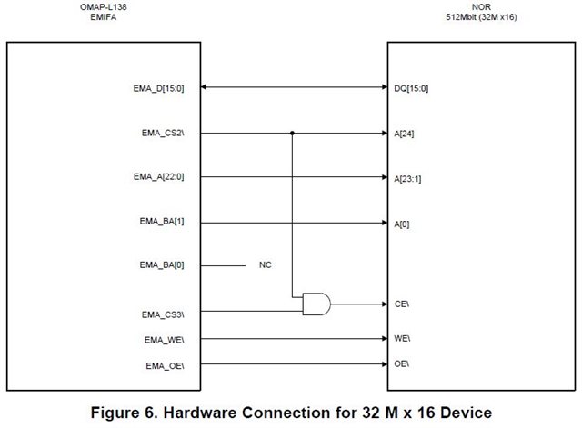
However, according to SPRS377F.pdf, the datasheet for TMS320C6745, 6747,

the only address pins assigned to the EMIFA are two bank address pins and 13 address pins, with no other multiplexed pins appearing.

I wonder if the aforementioned interface connection is really possible.

Pleas check it for me.

Thanks.

  • Hi,

    Sorry for the delay.

    A 64MB NOR flash can be booted from using a 2-stage bootloader:
    Stage 1: Primary bootloader - ROM code copies upto 32KB from lowest addresses of NOR flash. Within this 32KB is second stage bootloader.
    Stage 2: Second stage bootloader - software addresses > 32KB of flash by setting GPIOs before each EMIFA accesses and/or by accessing multiple chip selects with AND gate glue logic. The extra GPIOS and/or chip selects map to upper address bits allowing access > 32KB.

    C6747 EMIFA has 15 address bits (pins A[12:0] + BA[1:0]) that can access 32KB per chip select (4 CS). The primary bootloader in ROM code will therefore be limited to accessing upto 32KB on EMA_CS[2]. This program (32KB or smaller) will be copied into internal memory and executed. The software contents of this program must implement a second stage bootloader which can be programmed to copy additional content from the EMIFA-connected device.

    Since the software is completely in your control, GPIOs can be configured before each EMIFA read access. This allows utilization of all address bits of the NOR flash.
    The only requirement is that the GPIOs reset to a known state (usually 0V with external pull-down resistors) so that the primary bootloader always accesses the same addresses of NOR flash (usually the lowest addresses). Keep in mind that the memory map for EMIFA asynch chip selects (CS2, CS3, CS4, CS5) can access up to 32MB. The secondary bootloader will repeatedly access the lowest 32KB, but the NOR flash will be addressing > 32KB when the GPIOs mapped to upper address bits are non-zero.

    Alternately, the secondary bootloader can exploit unused chip selects to access > 32KB of data/program from the NOR flash. The primary bootloader always uses CS2 - driving it low during accesses. When the secondary bootloader accesses CS3, CS4, or CS5, AND gate logic is used to map each CS to upper address bits that cannot be reached by the EMIFA address bus. Similarly, whenver any of the CS is driven low (only one will be low at any time), AND gate logic must assert the CS pin on the NOR flash low also. Refer to SPRACK9 Figure 8. Hardware Connection for 64 M x 16 Device (below).

    Finally, an explanation of BA[1:0] in address: EMA_A[0] always provides the least significant bit of a 32-bit word address. Therefore, when interfacing to a 16-bit or 8-bit asynchronous device, the EMA_BA[1] and EMA_BA[0] pins provide the least-significant bits of the halfword or byte address, respectively.

    Regards,
    Mark

  • Hello, Mark.

    First of all, thanks for your kind explanation.

    Most of my questions were resolved, and I proceeded with the design as follows.

    1) NOR flash storing the booting image has been changed to 16MB.

    2) Allocate Bank 4 GPIO[0:9) for EMA_A[13:22] and put them to be pulled down to GND with 1k resistors as upper address pins for more than 32KB.

    Actually, In my system, there are 4 external memory ICs: NOR flash (16MB), FPGA, 1553B IC (only RT), and Asynchronous Non-volatile RAMs (8MB (4MB x 2EA)).

    And then, CS areas for them are as follows:

    CS0 - FPGA

    CS2 - NOR flash

    CS3 - 1553B

    CS4 - Non-volatile RAM#1

    CS5 - Non-volatile RAM#2

    Another question arises here.

    1) CS0 is for SDRAM, and I think it would be possible to allocate the FPGA at CS0 if setting the FPGA to read or write synchronously like SDRAM.

        Is this correct?

    2) The required capacity for non-volatile memory is 8MB, and I will use two 4MB NVRAMs (non-volatile RAM).

        I think it would be possible to allocate these two NVRAM at the same CS area, which means that CS pin and MSBs (A[22] and A[21]) are wired oring

        by OR gate logic.

        For example, NVRAM#1 is selected when CS pin and A[22] are logic low and [A21] is logic high, NVRAM#2 is selected when CS pin and A[21] are logic

        low and [A22] is logic high.

        Is this correct?

    Best Regards,

    Youngho.


  • Hi Youmgho,

    Appreciate you sharing the details.

    1) NOR flash storing the booting image has been changed to 16MB.

    Okay. The primary bootloader copies upto 32KB from lowest addresses of NOR flash

    2) Allocate Bank 4 GPIO[0:9) for EMA_A[13:22] and put them to be pulled down to GND with 1k resistors as upper address pins for more than 32KB.

    Okay. ZKB package supports all the chip selects. Watch out for reduced performance with so many loads.
    What clock rate are you targeting for the FPGA SDRAM interface?
    The datasheet does not seem to specify any assumed range of load capacitance for timing closure, but it does offer this note:

    https://www.ti.com/lit/ds/symlink/tms320c6745.pdf

    6.10.3 EMIFA SDRAM Loading Limitations
    EMIFA supports SDRAM up to 100 MHz with up to two SDRAM or asynchronous memory loads.
    Additional loads will limit the SDRAM operation to lower speeds and the maximum speed should be confirmed by board simulation using IBIS models.

    Your system must satisfy 6.10.6 EMIFA Electrical Data/Timing and any requirements from the FPGA + memories. Large loads and traces connecting these loads will slow signal propagation down and may cause unwanted signal reflections too.

    You could put the FPGA on EMIFB SDRAM interface if you can afford the pins.

    In either case, the FPGA will have to behave like one of the supported SDRAM configurations.
    Table 6-17. EMIFA Supported SDRAM Configurations
    Table 6-23. EMIFB Supported SDRAM Configurations

    Choose carefully the GPIOs you assign to be upper address pins.

    For example, Bank 4 GPIO[0:9) for EMA_A[13:22] includes BOOT[12] which will need to be high or low depending on the boot mode. Often external resistors are used, but a buffer could also assert boot mode signals until a short time after reset is released.
    BOOT[12] also has an internal pull-up (IPU). So size any pull-down resistor large enough to avoid holding the voltage between VIH and VIL. The IPU will be in contention with external 1k pull down.

    Check all the pin IPD/IPU status during reset in Datasheet section 3.6 Terminal Functions.

    1) CS0 is for SDRAM, and I think it would be possible to allocate the FPGA at CS0 if setting the FPGA to read or write synchronously like SDRAM.

    Its possible to have an FPGA emulate SDRAM. EMIFA does not support Mobile SDRAM devices. See comments above.

    2) The required capacity for non-volatile memory is 8MB, and I will use two 4MB NVRAMs (non-volatile RAM).

    The OR gate logic should work as described if you use OR logic gates. Consider pin voltage level during and after reset until software configures them.

    These MSBs (A[22] and A[21]) will be driven by GPIOs, controlled by software anyway. Avoid having both GPIOs low at the same time or both devices could be selected! You might throw additional logic to prevent this in hardware -  (A[22] NOR A[21]) as an additional input into the OR-gate to each CS maybe... lots of options.
    Recommend you confirm software can meet your latency/bandwidth requirements since GPIOs are required to change between EMIF accesses.

    "wired oring" to me means shorted together, like the I2C bus with its open-drain outputs that either release the bus to float or connect the bus to GND.
    Don't short CS to any addr pins with EMIF signals! Use discrete gate logic.

    Regards,
    Mark