This thread has been locked.

If you have a related question, please click the "Ask a related question" button in the top right corner. The newly created question will be automatically linked to this question.

TMS320C6748: About FSXM/FSRM bit of the McASP Frame Sync Generator

Part Number: TMS320C6748
Other Parts Discussed in Thread: PCM1808

In SPRUH79C 23.0.21.3 Frame Sync Generator,It says:

-------------------------

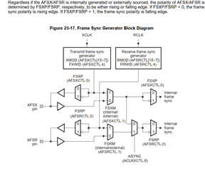
Regardless if the AFSX/AFSR is internally generated or externally sourced, the polarity of AFSX/AFSR is
determined by FSXP/FSRP, respectively, to be either rising or falling edge. If FSXP/FSRP = 0, the frame
sync polarity is rising edge. If FSXP/FSRP = 1, the frame sync polarity is falling edge.

-------------------------

If the AFSR polarity is a falling edge, as in the I2S format, set the FSRP bit to 1.

At this time, if FSRM = 1, "Internal frame sync" will fall at the beginning of the frame.

On the other hand, if FSRM = 0, "Internal frame sync" will rise at the beginning of the frame.

This behavior is considered to be inconsistent with the comments above.

  • Hi Hiroshi-san,

    How are you observing the internal internal frame sync? I think you must route it to the AFSX/AFSR pin as an output.

    Are you observing these signals with an oscilloscope?

    What is the clock source for both cases when FSRM = 1 and FSRM = 0?

    When FSRM = 0, AFSX/AFSR from internal source, the McASP generates the AFSX/AFSR signal from the internal or exernal ACLKX/ACLKR clock source. I want to ensure this is configured as you expect.

    What frequency is the bit clock ACLKX/ACLKR when sourced internally and externally?

    Refer to appnote sprack0 section 5.1 How Do I Configure a McASP for I2S Mode.

    Regards,
    Mark

  • Hi Mark ,

    We are currently manufacturing printed circuit boards. And we are designing software.

    We can't observe the signal yet.

    Our board has an ADC PCM1808(receive only) which in slave mode.

    The AHCLKR, ACLKR and ASFR are output of McASP.

    What is the clock source for both cases when FSRM = 1 and FSRM = 0?

    The clock source for both cases is internal RCLK.

    I am thinking of setting FSRM=0 because the internal frame sync is synchronized with the external ADC.

    Because I think that 

    when FSRM=1 , the polarity of the external ADC will be falling edge and  the polarity of the internal frame sync signal will be rising edge. 

    FSRM=0:  left FSRP inverter -> AFSR pin -> FSRM MUX -> ASYNC MUX -> FSRP inverter: two inverters.

    FSRM=1:  FSRM MUX -> ASYNC MUX -> FSRP inverter: one inverter.

    When is the setting of FSRM = 1 useful?


    When FSRM = 0, AFSX/AFSR from internal source, the McASP generates the AFSX/AFSR signal from the internal or exernal ACLKX/ACLKR clock source. I want to ensure this is configured as you expect.

    I think so too.

    Regards,

    Hiroshi

  • Hiroshi-san,

    I will get back to you about this on Monday.

    Regards,
    Mark

  • Hi Hiroshi-san,

    Sorry for taking so long.

    when FSRM=1 , the polarity of the external ADC will be falling edge and  the polarity of the internal frame sync signal will be rising edge. 

    FSRM=0:  left FSRP inverter -> AFSR pin -> FSRM MUX -> ASYNC MUX -> FSRP inverter: two inverters.

    FSRM=1:  FSRM MUX -> ASYNC MUX -> FSRP inverter: one inverter.

    No, See attached drawings showing the possible paths of the FSR signal for FSRP=1,FSRM=0/1. The path you have described is not a valid path. The pin direction determines if the output buffer or input buffer is used. Never will output buffer loop back into the input buffer with this AFSR signal. There will never be two inverters in the FSR path. I have corrected the statement below.

    FSRM=0:  AFSR pin -> FSRM MUX -> ASYNC MUX -> FSRP inverter: one inverter.
                     Frame Sync from EXTERNAL source: signal from from pin through input buffer to the internal frame sync

    FSRM=1:  FSRM MUX -> ASYNC MUX -> FSRP inverter: one inverter.
                     Frame Sync from INTERNAL source: signal from receive frame sync generator branches to two places: 1) to the output buffer and pin 2) to the internal frame sync


    Figure 19 in the datasheet for the PCM1808 shows "Master mode" with FSYNC launching on the rising BCLK edge (PCM1808 generates BCLK/FSYNC).

    However, in "Slave mode", the PCM1808 obeys the I2S protocol: MSB data in 2nd cycle after falling edge of FSYNC. Figure 18 in PCM1808 datasheet shows FSYNC transitioning on FALLING edge of BCLK.

    For your case where you are using the McASP to generate the BCLK and FSYNC to the PCM1808.
    Set AFSRCTL.FSRM = 1: Internally-generated receive frame sync.
    Set AFSRCTL.FSRP to 1: A falling edge on receive frame sync (AFSR) indicates the beginning of a frame.
    Set RFMT.RDATDLY to 1 for 1-bit data delay with respect to the frame sync.
    Set AFSRCTL.RMOD to 2 for 2-slot TDM (I2S mode).
    Set rest of bits according to word length
    Set PDIR[31] = 1 for AFSR Pin direction as output
    Possibly set RXACTIVE[0] = 0 LVCMOS receivers are disabled for pin group 0 (AFSR is in CP[0]). Check if ALL pins in pin group 0 can turn off receiver. See 3.7 Terminal Functions table in datasheet.
    Follow sequence in 23.0.21.1.2 Transmit/Receive Section Initialization with special attention to reading back GBLCTL.

    Regards,
    Mark

  • Hi Mark,

    Thank you for long polite answer.

    In SPRUH79C 23.0.21.6.1 it says:

    This hinted me that  ASFR pin also may  be routed back to the McASP.

    If FSRM=1 and FSRP=1,I have a question:

    The ADC will recognize that ASFR falling edge is beginnig of the flame.

    And "Internal frame sync" signal falling edge also must be beginning of the flame.

    How the internal logic know if "Internal frame sync" polarity is rising or falling? FSRP bit ?

    In FSRP=0 system, "Internal frame sync" polarity must be rising edge and

    in FSRP=1 system, "Internal frame sync" polarity must be falling edge?

    I think "Internal frame sync" signal polarity must be always rising edge.

    I can understand it if it looks like the figure below.

    regards,

    Hiroshi.

  • Hi Hiroshi-san,

    You make a valid point. Let me double check with the designer that the polarity muxes in this figure actually represent the hardware accurately.

    I agree that pad-loopback AFSR can reduce skew between AFSR and received data. I will check if the effects on AFSR polarity was fully considered in that mode. pad-loopback AFSR input will be delayed by AFSR output buffer + AFSR input buffer, reducing skew to the data that is delayed by the clock through its output buffer + board trace + data from codec output buffer + board trace + McASP input buffer. I suppose you might also pad-loopback ACLKR. Input/ output buffer delays are process dependent and vary with temperature. One way to reduce worst case of this variable delay is to delay clock (and frame sync I suppose) with the same delay - by using pad-loopback on these inputs.

    I think "Internal frame sync" polarity is rising edge too - and that is why the inverters exist before the signal reaches it. I'll try to confirm all of this. Give me a few days.

    Regards,
    Mark

  • Hi Hiroshi-san,

    A quick update: I found a slightly different figure in the internal McASP spec (below). This figure shows only one FSRP mux (instead of two) with one input that inverts the polarity of AFSR before it goes to "Internal frame sync". To prove which figure is accurate (TRM or internal spec), we need to enable pad loopback and then probe the signals with both FSRP = 1 and FSRP = 0 to check for any possible effects of the AFSR signal being inverted twice before getting to the "Internal frame sync" logic.

    Again, with the PCM1808 the pad-loop-back feature for AFSR is not too useful because the max clock rate of ~12Mhz is relatively slow.

    Regards,
    Mark