This thread has been locked.

If you have a related question, please click the "Ask a related question" button in the top right corner. The newly created question will be automatically linked to this question.

TDA4VM: /sys/kernel/debug/gpio information does not match configuration in dts

Part Number: TDA4VM

Hi TI Group,

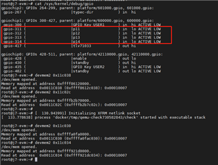
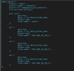
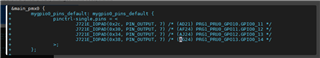
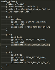
I configure the dts as below screenshot1 shown, then re-build the linux kernel and replace the old .dtb files with the new ones, but I found the /sys/kernel/debug/gpio information does not match configuration in dts,it should be output-high expectantly. Besides,the line-name of /sys/kernel/debug/gpio is also not correct,please help to check, thanks in advance.

k3-j721e-common-proc-board.dts:

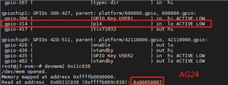
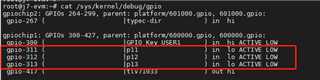
/sys/kernel/debug/gpio:

Best Regards

  • Hi,

    What is the physical status of those lines? Are they actually high? Have you measured the same via oscilloscope?
    Check the pin mux of all the pins.

    Best Regards,
    Keerthy

  • Hi,

    What is the physical status of those lines? Are they actually high? Have you measured the same via oscilloscope?
    Check the pin mux of all the pins.

    yes, I have measured them via oscilloscope, and they keep in low and no output. 

  • Hi Veitch,

    It must be issue with the pinmux settings. Can you please share the register values of all the pinmux registers for the GPIO you are configuring?

    Best Regards,
    Keerthy

  • Hi Keerthy,

    These are the register values of the GPIOs:

    All of the register values are 0x00010007, meaning PIN_GPIO_INPUT I think. And in other to verifiy your assumtion  "It must be issue with the pinmux settings",  I have tried to remove all the other cores firmware in /lib/firmware, just to run A72 only, but all the gpios' register values are still 0x00010007, nothing change.

  • Hi Veitch,

    Can you try this from Linux command prompt:

    devmem2 0x11C02C w 0x08050007

    Bit18 has to be set:


    Similarly for the other pin mux registers & let me know if you can see the GPIO lines toggling physically.

    If that helps please click on verify answer.

    Best Regards,
    Keerthy

  • Hi Keerthy,

    It will work with operating the register directly, but I need to make it work with dts configuration, that's the point I think.

  • Veitch,

    Refer: "arch/arm64/boot/dts/ti/k3-j721e-common-proc-board.dts"

    sw10_button_pins_default: sw10-button-pins-default {
    pinctrl-single,pins = <
    J721E_IOPAD(0x0, PIN_INPUT, 7) /* (AC18) EXTINTn.GPIO0_0 */
    >;
    };

    So your pins that need to be controlled as GPIOs need to be defined as above for pin mux. Follow the above settings for the pins
    that you want as GPIOs. Then the hardware will toggle as expected.

    If no further questions please click on verify answer.

    - Keerthy

  • Hi Keerthy,

    The issue persists, could you please help to check the attached dts&pinmux file? thanksJ721E_Pinmux_dts.zip

  • Hi Veitch,

    The zip is huge. Just share the code changes as a patch that was done to enable GPIO & Pinmux.

    I want to particularly review the pinmux changes.

    Regards,
    Keerthy

  • Hi Keerthy,

    Currently I‘m not sure whether there's an overwriten issue happens, thus, I attach both two patches about dts & pinmux,  you could focus on the below 4 GPIOs(AD21,AF24,AG24,AJ24) changes in the code, thanks

    dts patch:

    diff -Nuar default_linux_dts/k3-j721e-common-proc-board.dts linux_dts/k3-j721e-common-proc-board.dts
    --- default_linux_dts/k3-j721e-common-proc-board.dts	2021-08-05 06:28:09.000000000 +0800
    +++ linux_dts/k3-j721e-common-proc-board.dts	2021-11-16 15:27:43.352290666 +0800
    @@ -22,17 +22,18 @@
     		autorepeat;
     		pinctrl-names = "default";
     		pinctrl-0 = <&sw10_button_pins_default &sw11_button_pins_default>;
    -
    +		
     		sw10: sw10 {
    -			label = "GPIO Key USER1";
    -			linux,code = <BTN_0>;
    -			gpios = <&main_gpio0 0 GPIO_ACTIVE_LOW>;
    +
    +		        label = "GPIO Key USER1";
    +		        linux,code = <BTN_0>;
    +		        gpios = <&main_gpio0 0 GPIO_ACTIVE_LOW>;
     		};
     
     		sw11: sw11 {
    -			label = "GPIO Key USER2";
    -			linux,code = <BTN_1>;
    -			gpios = <&wkup_gpio0 7 GPIO_ACTIVE_LOW>;
    +		        label = "GPIO Key USER2";
    +		        linux,code = <BTN_1>;
    +		        gpios = <&wkup_gpio0 7 GPIO_ACTIVE_LOW>;
     		};
     	};
     
    @@ -187,6 +188,22 @@
     };
     
     &main_pmx0 {
    +	mygpio0_pins_default: mygpio0_pins_default {
    +		pinctrl-single,pins = <
    +			J721E_IOPAD(0x2c, PIN_OUTPUT, 7) /* (AD21) PRG1_PRU0_GPO10.GPIO0_11 */
    +			J721E_IOPAD(0x30, PIN_OUTPUT, 7) /* (AF24) PRG1_PRU0_GPO11.GPIO0_12 */
    +			J721E_IOPAD(0x34, PIN_OUTPUT, 7) /* (AJ24) PRG1_PRU0_GPO12.GPIO0_13 */
    +			J721E_IOPAD(0x38, PIN_OUTPUT, 7) /* (AG24) PRG1_PRU0_GPO13.GPIO0_14 */
    +		>;
    +	};
    +
    +	myuart1_pins_default: myuart1_pins_default {
    +		pinctrl-single,pins = <
    +			J721E_IOPAD(0x1f8, PIN_INPUT, 0) /* (AA4) UART1_RXD */
    +			J721E_IOPAD(0x1fc, PIN_OUTPUT_PULLUP, 0) /* (AB4) UART1_TXD */
    +		>;
    +	};
    +
     	sw10_button_pins_default: sw10-button-pins-default {
     		pinctrl-single,pins = <
     			J721E_IOPAD(0x0, PIN_INPUT, 7) /* (AC18) EXTINTn.GPIO0_0 */
    @@ -375,6 +392,13 @@
     	power-domains = <&k3_pds 146 TI_SCI_PD_SHARED>;
     };
     
    +&main_uart1 {
    + 	pinctrl-names = "default";
    +   	pinctrl-0 = <&myuart1_pins_default>;
    +    	status = "okay";
    +};
    +
    +
     &main_uart3 {
     	/* UART not brought out */
     	status = "disabled";
    @@ -405,6 +429,41 @@
     	status = "disabled";
     };
     
    +&main_gpio0 {
    +	status = "okay";
    +	pinctrl-names = "default";
    +	pinctrl-0 = <&mygpio0_pins_default>;
    +	//ti,no-reset-on-init;
    +
    +	p14: p14 {
    +		gpio-hog;
    +		gpios = <14 GPIO_ACTIVE_LOW>;
    +		output-high;
    +		lines-name = "AG24";
    +	};
    +
    +	p11 {
    +		gpio-hog;
    +		gpios = <11 GPIO_ACTIVE_LOW>;
    +		output-high;
    +		lines-name = "DES_PWR_3V3_EN_1";
    +	};
    +
    +	p12 {
    +		gpio-hog;
    +		gpios = <12 GPIO_ACTIVE_LOW>;
    +		output-high;
    +		lines-name = "DES_PWR_3V3_EN_2";
    +	};
    +
    +	p13 {
    +		gpio-hog;
    +		gpios = <13 GPIO_ACTIVE_LOW>;
    +		output-high;
    +		lines-name = "DES_PWR_3V3_EN_3";
    +	};
    +};
    +
     &main_gpio2 {
     	status = "disabled";
     };
    @@ -442,8 +501,8 @@
     
     &main_sdhci1 {
     	/* SD/MMC */
    -	vmmc-supply = <&vdd_mmc1>;
    -	vqmmc-supply = <&vdd_sd_dv_alt>;
    +	//vmmc-supply = <&vdd_mmc1>;
    +	//vqmmc-supply = <&vdd_sd_dv_alt>;
     	pinctrl-names = "default";
     	pinctrl-0 = <&main_mmc1_pins_default>;
     	ti,driver-strength-ohm = <50>;
    @@ -490,10 +549,12 @@
     };
     
     &usb0 {
    -	dr_mode = "otg";
    -	maximum-speed = "super-speed";
    -	phys = <&serdes3_usb_link>;
    -	phy-names = "cdns3,usb3-phy";
    +	dr_mode = "host";
    +    maximum-speed = "high-speed";
    +	//dr_mode = "otg";
    +	//maximum-speed = "super-speed";
    +	//phys = <&serdes3_usb_link>;
    +	//phy-names = "cdns3,usb3-phy";
     };
     
     &usbss1 {
    diff -Nuar default_linux_dts/k3-j721e-common-proc-board-infotainment.dts linux_dts/k3-j721e-common-proc-board-infotainment.dts
    --- default_linux_dts/k3-j721e-common-proc-board-infotainment.dts	2021-08-05 06:27:50.000000000 +0800
    +++ linux_dts/k3-j721e-common-proc-board-infotainment.dts	2021-11-16 15:23:09.953473762 +0800
    @@ -78,7 +78,7 @@
     			J721E_IOPAD(0x5c, PIN_OUTPUT, 10) /* (AG23) PRG1_PRU1_GPO1.VOUT0_DATA1 */
     			J721E_IOPAD(0x60, PIN_OUTPUT, 10) /* (AF23) PRG1_PRU1_GPO2.VOUT0_DATA2 */
     			J721E_IOPAD(0x64, PIN_OUTPUT, 10) /* (AD23) PRG1_PRU1_GPO3.VOUT0_DATA3 */
    -			J721E_IOPAD(0x68, PIN_OUTPUT, 10) /* (AH24) PRG1_PRU1_GPO4.VOUT0_DATA4 */
    +			//J721E_IOPAD(0x68, PIN_OUTPUT, 10) /* (AH24) PRG1_PRU1_GPO4.VOUT0_DATA4 */
     			J721E_IOPAD(0x6c, PIN_OUTPUT, 10) /* (AG21) PRG1_PRU1_GPO5.VOUT0_DATA5 */
     			J721E_IOPAD(0x70, PIN_OUTPUT, 10) /* (AE23) PRG1_PRU1_GPO6.VOUT0_DATA6 */
     			J721E_IOPAD(0x74, PIN_OUTPUT, 10) /* (AC21) PRG1_PRU1_GPO7.VOUT0_DATA7 */
    @@ -92,7 +92,7 @@
     			J721E_IOPAD(0x94, PIN_OUTPUT, 10) /* (AJ27) PRG1_PRU1_GPO15.VOUT0_DATA15 */
     			J721E_IOPAD(0x30, PIN_OUTPUT, 10) /* (AF24) PRG1_PRU0_GPO11.VOUT0_DATA16 */
     			J721E_IOPAD(0x34, PIN_OUTPUT, 10) /* (AJ24) PRG1_PRU0_GPO12.VOUT0_DATA17 */
    -			J721E_IOPAD(0x38, PIN_OUTPUT, 10) /* (AG24) PRG1_PRU0_GPO13.VOUT0_DATA18 */
    +			//J721E_IOPAD(0x38, PIN_OUTPUT, 10) /* (AG24) PRG1_PRU0_GPO13.VOUT0_DATA18 */
     			J721E_IOPAD(0x3c, PIN_OUTPUT, 10) /* (AD24) PRG1_PRU0_GPO14.VOUT0_DATA19 */
     			J721E_IOPAD(0x40, PIN_OUTPUT, 10) /* (AC24) PRG1_PRU0_GPO15.VOUT0_DATA20 */
     			J721E_IOPAD(0x44, PIN_OUTPUT, 10) /* (AE24) PRG1_PRU0_GPO16.VOUT0_DATA21 */
    diff -Nuar default_linux_dts/k3-j721e-eaik.dts linux_dts/k3-j721e-eaik.dts
    --- default_linux_dts/k3-j721e-eaik.dts	2021-08-05 06:27:50.000000000 +0800
    +++ linux_dts/k3-j721e-eaik.dts	2021-11-16 15:23:09.957473786 +0800
    @@ -426,7 +426,7 @@
     			J721E_IOPAD(0x5c, PIN_OUTPUT, 10) /* (AG23) PRG1_PRU1_GPO1.VOUT0_DATA1 */
     			J721E_IOPAD(0x60, PIN_OUTPUT, 10) /* (AF23) PRG1_PRU1_GPO2.VOUT0_DATA2 */
     			J721E_IOPAD(0x64, PIN_OUTPUT, 10) /* (AD23) PRG1_PRU1_GPO3.VOUT0_DATA3 */
    -			J721E_IOPAD(0x68, PIN_OUTPUT, 10) /* (AH24) PRG1_PRU1_GPO4.VOUT0_DATA4 */
    +			//J721E_IOPAD(0x68, PIN_OUTPUT, 10) /* (AH24) PRG1_PRU1_GPO4.VOUT0_DATA4 */
     			J721E_IOPAD(0x6c, PIN_OUTPUT, 10) /* (AG21) PRG1_PRU1_GPO5.VOUT0_DATA5 */
     			J721E_IOPAD(0x70, PIN_OUTPUT, 10) /* (AE23) PRG1_PRU1_GPO6.VOUT0_DATA6 */
     			J721E_IOPAD(0x74, PIN_OUTPUT, 10) /* (AC21) PRG1_PRU1_GPO7.VOUT0_DATA7 */
    @@ -440,7 +440,7 @@
     			J721E_IOPAD(0x94, PIN_OUTPUT, 10) /* (AJ27) PRG1_PRU1_GPO15.VOUT0_DATA15 */
     			J721E_IOPAD(0x30, PIN_OUTPUT, 10) /* (AF24) PRG1_PRU0_GPO11.VOUT0_DATA16 */
     			J721E_IOPAD(0x34, PIN_OUTPUT, 10) /* (AJ24) PRG1_PRU0_GPO12.VOUT0_DATA17 */
    -			J721E_IOPAD(0x38, PIN_OUTPUT, 10) /* (AG24) PRG1_PRU0_GPO13.VOUT0_DATA18 */
    +			//J721E_IOPAD(0x38, PIN_OUTPUT, 10) /* (AG24) PRG1_PRU0_GPO13.VOUT0_DATA18 */
     			J721E_IOPAD(0x3c, PIN_OUTPUT, 10) /* (AD24) PRG1_PRU0_GPO14.VOUT0_DATA19 */
     			J721E_IOPAD(0x40, PIN_OUTPUT, 10) /* (AC24) PRG1_PRU0_GPO15.VOUT0_DATA20 */
     			J721E_IOPAD(0x44, PIN_OUTPUT, 10) /* (AE24) PRG1_PRU0_GPO16.VOUT0_DATA21 */
    @@ -608,8 +608,8 @@
     
     &main_sdhci1 {
     	/* SD Card */
    -	vmmc-supply = <&vdd_mmc1>;
    -	vqmmc-supply = <&vdd_sd_dv_alt>;
    +	//vmmc-supply = <&vdd_mmc1>;
    +	//vqmmc-supply = <&vdd_sd_dv_alt>;
     	pinctrl-names = "default";
     	pinctrl-0 = <&main_mmc1_pins_default>;
     	ti,driver-strength-ohm = <50>;
    diff -Nuar default_linux_dts/k3-j721e-main.dtsi linux_dts/k3-j721e-main.dtsi
    --- default_linux_dts/k3-j721e-main.dtsi	2021-08-05 06:28:13.000000000 +0800
    +++ linux_dts/k3-j721e-main.dtsi	2021-11-16 15:23:09.961473811 +0800
    @@ -1176,13 +1176,13 @@
     		assigned-clocks = <&k3_clks 91 1>;
     		assigned-clock-parents = <&k3_clks 91 2>;
     		bus-width = <8>;
    -		mmc-hs400-1_8v;
    +		//mmc-hs400-1_8v;
     		mmc-ddr-1_8v;
     		ti,otap-del-sel-legacy = <0xf>;
     		ti,otap-del-sel-mmc-hs = <0xf>;
     		ti,otap-del-sel-ddr52 = <0x5>;
    -		ti,otap-del-sel-hs200 = <0x6>;
    -		ti,otap-del-sel-hs400 = <0x0>;
    +		//ti,otap-del-sel-hs200 = <0x6>;
    +		//ti,otap-del-sel-hs400 = <0x0>;
     		ti,trm-icp = <0x8>;
     		ti,strobe-sel = <0x77>;
     		dma-coherent;
    @@ -2124,7 +2124,7 @@
     		};
     	};
     
    -	timesync_router: timesync_router@A40000 {
    +	timesync_router: timesync_router@a40000 {
     		compatible = "pinctrl-single";
     		reg = <0x0 0xa40000 0x0 0x800>;
     		#address-cells = <1>;
    diff -Nuar default_linux_dts/k3-j721e-proc-board-tps65917.dts linux_dts/k3-j721e-proc-board-tps65917.dts
    --- default_linux_dts/k3-j721e-proc-board-tps65917.dts	2021-08-05 06:27:50.000000000 +0800
    +++ linux_dts/k3-j721e-proc-board-tps65917.dts	2021-11-16 15:23:09.969473860 +0800
    @@ -8,6 +8,7 @@
     #include "k3-j721e-common-proc-board.dts"
     
     &wkup_i2c0 {
    +	status="disabled";
     	pinctrl-names = "default";
     	pinctrl-0 = <&wkup_i2c0_pins_default>;
     	clock-frequency = <400000>;
    @@ -45,9 +46,9 @@
     	};
     };
     
    -&vdd_sd_dv_alt {
    -	status = "disabled";
    -};
    +//&vdd_sd_dv_alt {
    +//	status = "okay";
    +//};
     
     &main_sdhci1 {
     	vqmmc-supply = <&ldo1_reg>;
    

    pinmux patch:

    diff -Nuar default_rtos_pinmux/J721E_pinmux_data.c rtos_pinmux/J721E_pinmux_data.c
    --- default_rtos_pinmux/J721E_pinmux_data.c	2021-08-13 14:03:38.000000000 +0800
    +++ rtos_pinmux/J721E_pinmux_data.c	2021-11-16 15:26:27.414620480 +0800
    @@ -47,53 +47,198 @@
     };
     
     
    -static pinmuxPerCfg_t gDp0PinCfg[] =
    +static pinmuxPerCfg_t gGpio0PinCfg[] =
     {
    -    /* MyDP0 -> DP0_HPD -> Y4 */
    +     /* MyGPIO0 -> GPIO0_1 -> AC23 */
         {
    -        PIN_SPI0_CS1, PIN_MODE(5) | \
    +        PIN_PRG1_PRU0_GPO0, PIN_MODE(7) | \
             ((PIN_PULL_DISABLE | PIN_INPUT_ENABLE) & (~PIN_PULL_DIRECTION))
         },
    -    {PINMUX_END}
    -};
    -
    -static pinmuxModuleCfg_t gDpPinCfg[] =
    -{
    -    {0, TRUE, gDp0PinCfg},
    -    {PINMUX_END}
    -};
    -
    +    /* MyGPIO0 -> GPIO0_2 -> AG22 */
    +    {
    +        PIN_PRG1_PRU0_GPO1, PIN_MODE(7) | \
    +        ((PIN_PULL_DISABLE | PIN_INPUT_ENABLE) & (~PIN_PULL_DIRECTION))
    +    },
    +    /* MyGPIO0 -> GPIO0_3 -> AF22 */
    +    {
    +        PIN_PRG1_PRU0_GPO2, PIN_MODE(7) | \
    +        ((PIN_PULL_DISABLE | PIN_INPUT_ENABLE) & (~PIN_PULL_DIRECTION))
    +    },
    +    /* MyGPIO0 -> GPIO0_4 -> AJ23 */
    +    {
    +        PIN_PRG1_PRU0_GPO3, PIN_MODE(7) | \
    +        ((PIN_PULL_DISABLE | PIN_INPUT_ENABLE) & (~PIN_PULL_DIRECTION))
    +    },
    +    /* MyGPIO0 -> GPIO0_5 -> AH23 */
    +    {
    +        PIN_PRG1_PRU0_GPO4, PIN_MODE(7) | \
    +        ((PIN_PULL_DISABLE | PIN_INPUT_ENABLE) & (~PIN_PULL_DIRECTION))
    +    },
    +    /* MyGPIO0 -> GPIO0_7 -> AD22 */
    +    {
    +        PIN_PRG1_PRU0_GPO6, PIN_MODE(7) | \
    +        ((PIN_PULL_DISABLE | PIN_INPUT_ENABLE) & (~PIN_PULL_DIRECTION))
    +    },
    +    /* MyGPIO0 -> GPIO0_8 -> AE20 */
    +    {
    +        PIN_PRG1_PRU0_GPO7, PIN_MODE(7) | \
    +        ((PIN_PULL_DISABLE | PIN_INPUT_ENABLE) & (~PIN_PULL_DIRECTION))
    +    },
    +    /* MyGPIO0 -> GPIO0_9 -> AJ20 */
    +    {
    +        PIN_PRG1_PRU0_GPO8, PIN_MODE(7) | \
    +        ((PIN_PULL_DISABLE | PIN_INPUT_ENABLE) & (~PIN_PULL_DIRECTION))
    +    },
    +    /* MyGPIO0 -> GPIO0_10 -> AG20 */
    +    {
    +        PIN_PRG1_PRU0_GPO9, PIN_MODE(7) | \
    +        ((PIN_PULL_DISABLE | PIN_INPUT_ENABLE) & (~PIN_PULL_DIRECTION))
    +    },
    +    /* MyGPIO0 -> GPIO0_11 -> AD21 */
    +    {
    +        PIN_PRG1_PRU0_GPO10, PIN_MODE(7) | \
    +        ((PIN_PULL_DISABLE) & (~PIN_PULL_DIRECTION & ~PIN_INPUT_ENABLE))
    +    },
    +    /* MyGPIO0 -> GPIO0_12 -> AF24 */
    +    {
    +        PIN_PRG1_PRU0_GPO11, PIN_MODE(7) | \
    +        ((PIN_PULL_DISABLE) & (~PIN_PULL_DIRECTION & ~PIN_INPUT_ENABLE))
    +    },
    +    /* MyGPIO0 -> GPIO0_13 -> AJ24 */
    +    {
    +        PIN_PRG1_PRU0_GPO12, PIN_MODE(7) | \
    +        ((PIN_PULL_DISABLE) & (~PIN_PULL_DIRECTION & ~PIN_INPUT_ENABLE))
    +    },
     
    -static pinmuxPerCfg_t gGpio0PinCfg[] =
    -{
    -    /* MySYSTEM1 -> GPIO0_0 -> AC18 */
    +    /* MyGPIO0 -> GPIO0_14 -> AG24 */
    +    {
    +        PIN_PRG1_PRU0_GPO13, PIN_MODE(7) | \
    +        ((PIN_PULL_DISABLE) & (~PIN_PULL_DIRECTION & ~PIN_INPUT_ENABLE))
    +    },
    +    /* MyGPIO0 -> GPIO0_15 -> AD24 */
    +    {
    +        PIN_PRG1_PRU0_GPO14, PIN_MODE(7) | \
    +        ((PIN_PULL_DISABLE) & (~PIN_PULL_DIRECTION & ~PIN_INPUT_ENABLE))
    +    },
    +    /* MyGPIO0 -> GPIO0_16 -> AC24 */
    +    {
    +        PIN_PRG1_PRU0_GPO15, PIN_MODE(7) | \
    +        ((PIN_PULL_DISABLE | PIN_INPUT_ENABLE) & (~PIN_PULL_DIRECTION))
    +    },
    +    /* MyGPIO0 -> GPIO0_17 -> AE24 */
    +    {
    +        PIN_PRG1_PRU0_GPO16, PIN_MODE(7) | \
    +        ((PIN_PULL_DISABLE) & (~PIN_PULL_DIRECTION & ~PIN_INPUT_ENABLE))
    +    },
    +    /* MyGPIO0 -> GPIO0_18 -> AJ21 */
         {
    -        PIN_EXTINTN, PIN_MODE(7) | \
    +        PIN_PRG1_PRU0_GPO17, PIN_MODE(7) | \
             ((PIN_PULL_DISABLE | PIN_INPUT_ENABLE) & (~PIN_PULL_DIRECTION))
         },
    -    /* MyGPIO0 -> GPIO0_97 -> Y28 */
    +    /* MyGPIO0 -> GPIO0_19 -> AE21 */
    +    {
    +        PIN_PRG1_PRU0_GPO18, PIN_MODE(7) | \
    +        ((PIN_PULL_DISABLE) & (~PIN_PULL_DIRECTION & ~PIN_INPUT_ENABLE))
    +    },
    +    /* MyGPIO0 -> GPIO0_20 -> AH21 */
         {
    -        PIN_RGMII6_TX_CTL, PIN_MODE(7) | \
    +        PIN_PRG1_PRU0_GPO19, PIN_MODE(7) | \
             ((PIN_PULL_DISABLE | PIN_INPUT_ENABLE) & (~PIN_PULL_DIRECTION))
         },
    -    /* MyGPIO0 -> GPIO0_98 -> V23 */
    +    /* MyGPIO0 -> GPIO0_21 -> AE22 */
    +    {
    +        PIN_PRG1_PRU1_GPO0, PIN_MODE(7) | \
    +        ((PIN_PULL_DISABLE) & (~PIN_PULL_DIRECTION & ~PIN_INPUT_ENABLE))
    +    },
    +    /* MyGPIO0 -> GPIO0_22 -> AG23 */
    +    {
    +        PIN_PRG1_PRU1_GPO1, PIN_MODE(7) | \
    +        ((PIN_PULL_DISABLE) & (~PIN_PULL_DIRECTION & ~PIN_INPUT_ENABLE))
    +    },
    +    /* MyGPIO0 -> GPIO0_23 -> AF23 */
    +    {
    +        PIN_PRG1_PRU1_GPO2, PIN_MODE(7) | \
    +        ((PIN_PULL_DISABLE) & (~PIN_PULL_DIRECTION & ~PIN_INPUT_ENABLE))
    +    },
    +    /* MyGPIO0 -> GPIO0_24 -> AD23 */
    +    {
    +        PIN_PRG1_PRU1_GPO3, PIN_MODE(7) | \
    +        ((PIN_PULL_DISABLE) & (~PIN_PULL_DIRECTION & ~PIN_INPUT_ENABLE))
    +    },
    +    /* MyGPIO0 -> GPIO0_25 -> AH24 */
    +    {
    +        PIN_PRG1_PRU1_GPO4, PIN_MODE(7) | \
    +        ((PIN_PULL_DISABLE) & (~PIN_PULL_DIRECTION & ~PIN_INPUT_ENABLE))
    +    },
    +    /* MyGPIO0 -> GPIO0_26 -> AG21 */
    +    {
    +        PIN_PRG1_PRU1_GPO5, PIN_MODE(7) | \
    +        ((PIN_PULL_DISABLE) & (~PIN_PULL_DIRECTION & ~PIN_INPUT_ENABLE))
    +    },
    +    /* MyGPIO0 -> GPIO0_27 -> AE23 */
    +    {
    +        PIN_PRG1_PRU1_GPO6, PIN_MODE(7) | \
    +        ((PIN_PULL_DISABLE | PIN_INPUT_ENABLE) & (~PIN_PULL_DIRECTION))
    +    },
    +    /* MyGPIO0 -> GPIO0_32 -> AJ25 */
    +    {
    +        PIN_PRG1_PRU1_GPO11, PIN_MODE(7) | \
    +        ((PIN_PULL_DISABLE) & (~PIN_PULL_DIRECTION & ~PIN_INPUT_ENABLE))
    +    },
    +    /* MyGPIO0 -> GPIO0_43 -> AF28 */
    +    {
    +        PIN_PRG0_PRU0_GPO0, PIN_MODE(7) | \
    +        ((PIN_PULL_DISABLE) & (~PIN_PULL_DIRECTION & ~PIN_INPUT_ENABLE))
    +    },
    +    /* MyGPIO0 -> GPIO0_74 -> AG26 */
    +    {
    +        PIN_PRG0_PRU1_GPO11, PIN_MODE(7) | \
    +        ((PIN_PULL_DISABLE) & (~PIN_PULL_DIRECTION & ~PIN_INPUT_ENABLE))
    +    },
    +    /* MyGPIO0 -> GPIO0_78 -> AF29 */
         {
    -        PIN_RGMII6_RX_CTL, PIN_MODE(7) | \
    +        PIN_PRG0_PRU1_GPO15, PIN_MODE(7) | \
    +        ((PIN_PULL_DISABLE) & (~PIN_PULL_DIRECTION & ~PIN_INPUT_ENABLE))
    +    },
    +    /* MyGPIO0 -> GPIO0_79 -> AG29 */
    +    {
    +        PIN_PRG0_PRU1_GPO16, PIN_MODE(7) | \
    +        ((PIN_PULL_DISABLE) & (~PIN_PULL_DIRECTION & ~PIN_INPUT_ENABLE))
    +    },
    +    /* MyGPIO0 -> GPIO0_81 -> AA26 */
    +    {
    +        PIN_PRG0_PRU1_GPO18, PIN_MODE(7) | \
             ((PIN_PULL_DISABLE | PIN_INPUT_ENABLE) & (~PIN_PULL_DIRECTION))
         },
    -    /* MyGPIO0 -> GPIO0_117 -> W4 */
    +    /* MyGPIO0 -> GPIO0_82 -> AA29 */
         {
    -        PIN_SPI1_CS1, PIN_MODE(7) | \
    +        PIN_PRG0_PRU1_GPO19, PIN_MODE(7) | \
             ((PIN_PULL_DISABLE | PIN_INPUT_ENABLE) & (~PIN_PULL_DIRECTION))
         },
    -    /* MyGPIO0 -> GPIO0_127 -> AC4 */
    +    /* MyGPIO0 -> GPIO0_87 -> V28 */
         {
    -        PIN_UART1_CTSN, PIN_MODE(7) | \
    +        PIN_RGMII5_TD3, PIN_MODE(7) | \
    +        ((PIN_PULL_DISABLE) & (~PIN_PULL_DIRECTION & ~PIN_INPUT_ENABLE))
    +    },
    +    /* MyGPIO0 -> GPIO0_88 -> V29 */
    +    {
    +        PIN_RGMII5_TD2, PIN_MODE(7) | \
    +        ((PIN_PULL_DISABLE) & (~PIN_PULL_DIRECTION & ~PIN_INPUT_ENABLE))
    +    },
    +    /* MyGPIO0 -> GPIO0_89 -> V27 */
    +    {
    +        PIN_RGMII5_TD1, PIN_MODE(7) | \
             ((PIN_PULL_DISABLE | PIN_INPUT_ENABLE) & (~PIN_PULL_DIRECTION))
         },
    +    /* MyGPIO0 -> GPIO0_90 -> U28 */
    +    {
    +        PIN_RGMII5_TD0, PIN_MODE(7) | \
    +        ((PIN_PULL_DISABLE) & (~PIN_PULL_DIRECTION & ~PIN_INPUT_ENABLE))
    +    },
         {PINMUX_END}
     };
     
    +#if 0
     static pinmuxPerCfg_t gGpio1PinCfg[] =
     {
         /* MyGPIO1 -> GPIO1_0 -> AD5 */
    @@ -153,40 +298,27 @@
         },
         {PINMUX_END}
     };
    +#endif
     
     static pinmuxModuleCfg_t gGpioPinCfg[] =
     {
         {0, TRUE, gGpio0PinCfg},
    -    {1, TRUE, gGpio1PinCfg},
    +   // {1, TRUE, gGpio1PinCfg},
         {PINMUX_END}
     };
     
     
    -static pinmuxPerCfg_t gI2c2PinCfg[] =
    -{
    -    /* MyI2C2 -> I2C2_SCL -> AA1 */
    -    {
    -        PIN_SPI0_CLK, PIN_MODE(2) | \
    -        ((PIN_PULL_DIRECTION | PIN_INPUT_ENABLE) & (~PIN_PULL_DISABLE))
    -    },
    -    /* MyI2C2 -> I2C2_SDA -> AB5 */
    -    {
    -        PIN_SPI0_D0, PIN_MODE(2) | \
    -        ((PIN_PULL_DIRECTION | PIN_INPUT_ENABLE) & (~PIN_PULL_DISABLE))
    -    },
    -    {PINMUX_END}
    -};
     
     static pinmuxPerCfg_t gI2c6PinCfg[] =
     {
    -    /* MyI2C6 -> I2C6_SCL -> AA3 */
    +     /* MyI2C2 -> I2C6_SCL -> W2 */
         {
    -        PIN_SPI0_D1, PIN_MODE(2) | \
    +        PIN_I3C0_SCL, PIN_MODE(4) | \
             ((PIN_PULL_DIRECTION | PIN_INPUT_ENABLE) & (~PIN_PULL_DISABLE))
         },
    -    /* MyI2C6 -> I2C6_SDA -> Y2 */
    +    /* MyI2C2 -> I2C6_SDA -> W1 */
         {
    -        PIN_SPI1_D1, PIN_MODE(2) | \
    +        PIN_I3C0_SDA, PIN_MODE(4) | \
             ((PIN_PULL_DIRECTION | PIN_INPUT_ENABLE) & (~PIN_PULL_DISABLE))
         },
         {PINMUX_END}
    @@ -222,68 +354,15 @@
         {PINMUX_END}
     };
     
    -static pinmuxPerCfg_t gI2c3PinCfg[] =
    -{
    -    /* MyI2C3 -> I2C3_SCL -> T26 */
    -    {
    -        PIN_MMC2_CLK, PIN_MODE(4) | \
    -        ((PIN_PULL_DIRECTION | PIN_INPUT_ENABLE) & (~PIN_PULL_DISABLE))
    -    },
    -    /* MyI2C3 -> I2C3_SDA -> T25 */
    -    {
    -        PIN_MMC2_CMD, PIN_MODE(4) | \
    -        ((PIN_PULL_DIRECTION | PIN_INPUT_ENABLE) & (~PIN_PULL_DISABLE))
    -    },
    -    {PINMUX_END}
    -};
     
     static pinmuxModuleCfg_t gI2cPinCfg[] =
     {
    -    {2, TRUE, gI2c2PinCfg},
    -    {6, TRUE, gI2c6PinCfg},
         {0, TRUE, gI2c0PinCfg},
         {1, TRUE, gI2c1PinCfg},
    -    {3, TRUE, gI2c3PinCfg},
    -    {PINMUX_END}
    -};
    -
    -
    -static pinmuxPerCfg_t gMcan2PinCfg[] =
    -{
    -    /* MyMCAN2 -> MCAN2_RX -> AC2 */
    -    {
    -        PIN_UART0_CTSN, PIN_MODE(3) | \
    -        ((PIN_PULL_DISABLE | PIN_INPUT_ENABLE) & (~PIN_PULL_DIRECTION))
    -    },
    -    /* MyMCAN2 -> MCAN2_TX -> AB1 */
    -    {
    -        PIN_UART0_RTSN, PIN_MODE(3) | \
    -        ((PIN_PULL_DISABLE) & (~PIN_PULL_DIRECTION & ~PIN_INPUT_ENABLE))
    -    },
    -    {PINMUX_END}
    -};
    -
    -static pinmuxPerCfg_t gMcan0PinCfg[] =
    -{
    -    /* MyMCAN0 -> MCAN0_RX -> W5 */
    -    {
    -        PIN_MCAN0_RX, PIN_MODE(0) | \
    -        ((PIN_PULL_DISABLE | PIN_INPUT_ENABLE) & (~PIN_PULL_DIRECTION))
    -    },
    -    /* MyMCAN0 -> MCAN0_TX -> W6 */
    -    {
    -        PIN_MCAN0_TX, PIN_MODE(0) | \
    -        ((PIN_PULL_DISABLE) & (~PIN_PULL_DIRECTION & ~PIN_INPUT_ENABLE))
    -    },
    +    {6, TRUE, gI2c6PinCfg},
         {PINMUX_END}
     };
     
    -static pinmuxModuleCfg_t gMcanPinCfg[] =
    -{
    -    {2, TRUE, gMcan2PinCfg},
    -    {0, TRUE, gMcan0PinCfg},
    -    {PINMUX_END}
    -};
     
     
     static pinmuxPerCfg_t gMcu_i2c0PinCfg[] =
    @@ -308,93 +387,6 @@
     };
     
     
    -static pinmuxPerCfg_t gMcu_i3c0PinCfg[] =
    -{
    -    /* MyMCU_I3C0 -> MCU_I3C0_SCL -> D26 */
    -    {
    -        PIN_MCU_I3C0_SCL, PIN_MODE(0) | \
    -        ((PIN_PULL_DISABLE | PIN_INPUT_ENABLE) & (~PIN_PULL_DIRECTION))
    -    },
    -    /* MyMCU_I3C0 -> MCU_I3C0_SDA -> D25 */
    -    {
    -        PIN_MCU_I3C0_SDA, PIN_MODE(0) | \
    -        ((PIN_PULL_DISABLE | PIN_INPUT_ENABLE) & (~PIN_PULL_DIRECTION))
    -    },
    -    /* MyMCU_I3C0 -> MCU_I3C0_SDAPULLEN -> E26 */
    -    {
    -        PIN_PMIC_POWER_EN0, PIN_MODE(0) | \
    -        ((PIN_PULL_DISABLE) & (~PIN_PULL_DIRECTION & ~PIN_INPUT_ENABLE))
    -    },
    -    {PINMUX_END}
    -};
    -
    -static pinmuxModuleCfg_t gMcu_i3cPinCfg[] =
    -{
    -    {0, TRUE, gMcu_i3c0PinCfg},
    -    {PINMUX_END}
    -};
    -
    -
    -static pinmuxPerCfg_t gMcu_mcan0PinCfg[] =
    -{
    -    /* MyMCU_MCAN0 -> MCU_MCAN0_RX -> C29 */
    -    {
    -        PIN_MCU_MCAN0_RX, PIN_MODE(0) | \
    -        ((PIN_PULL_DISABLE | PIN_INPUT_ENABLE) & (~PIN_PULL_DIRECTION))
    -    },
    -    /* MyMCU_MCAN0 -> MCU_MCAN0_TX -> D29 */
    -    {
    -        PIN_MCU_MCAN0_TX, PIN_MODE(0) | \
    -        ((PIN_PULL_DISABLE) & (~PIN_PULL_DIRECTION & ~PIN_INPUT_ENABLE))
    -    },
    -    {PINMUX_END}
    -};
    -
    -static pinmuxPerCfg_t gMcu_mcan1PinCfg[] =
    -{
    -    /* MyMCU_MCAN1 -> MCU_MCAN1_RX -> G24 */
    -    {
    -        PIN_WKUP_GPIO0_5, PIN_MODE(0) | \
    -        ((PIN_PULL_DISABLE | PIN_INPUT_ENABLE) & (~PIN_PULL_DIRECTION))
    -    },
    -    /* MyMCU_MCAN1 -> MCU_MCAN1_TX -> G25 */
    -    {
    -        PIN_WKUP_GPIO0_4, PIN_MODE(0) | \
    -        ((PIN_PULL_DISABLE) & (~PIN_PULL_DIRECTION & ~PIN_INPUT_ENABLE))
    -    },
    -    {PINMUX_END}
    -};
    -
    -static pinmuxModuleCfg_t gMcu_mcanPinCfg[] =
    -{
    -    {0, TRUE, gMcu_mcan0PinCfg},
    -    {1, TRUE, gMcu_mcan1PinCfg},
    -    {PINMUX_END}
    -};
    -
    -
    -static pinmuxPerCfg_t gMcu_mdio0PinCfg[] =
    -{
    -    /* MyMCU_MDIO1 -> MCU_MDIO0_MDC -> F23 */
    -    {
    -        PIN_MCU_MDIO0_MDC, PIN_MODE(0) | \
    -        ((PIN_PULL_DISABLE) & (~PIN_PULL_DIRECTION & ~PIN_INPUT_ENABLE))
    -    },
    -    /* MyMCU_MDIO1 -> MCU_MDIO0_MDIO -> E23 */
    -    {
    -        PIN_MCU_MDIO0_MDIO, PIN_MODE(0) | \
    -        ((PIN_PULL_DISABLE | PIN_INPUT_ENABLE) & (~PIN_PULL_DIRECTION))
    -    },
    -    {PINMUX_END}
    -};
    -
    -static pinmuxModuleCfg_t gMcu_mdioPinCfg[] =
    -{
    -    {0, TRUE, gMcu_mdio0PinCfg},
    -    {PINMUX_END}
    -};
    -
    -
     static pinmuxPerCfg_t gMcu_fss0_ospi0PinCfg[] =
     {
         /* MyMCU_OSPI0 -> MCU_OSPI0_CLK -> E20 */
    @@ -455,55 +447,9 @@
         {PINMUX_END}
     };
     
    -static pinmuxPerCfg_t gMcu_fss0_ospi1PinCfg[] =
    -{
    -    /* MyMCU_OSPI1 -> MCU_OSPI1_CLK -> F22 */
    -    {
    -        PIN_MCU_OSPI1_CLK, PIN_MODE(0) | \
    -        ((PIN_PULL_DISABLE) & (~PIN_PULL_DIRECTION & ~PIN_INPUT_ENABLE))
    -    },
    -    /* MyMCU_OSPI1 -> MCU_OSPI1_CSn0 -> C22 */
    -    {
    -        PIN_MCU_OSPI1_CSN0, PIN_MODE(0) | \
    -        ((PIN_PULL_DISABLE) & (~PIN_PULL_DIRECTION & ~PIN_INPUT_ENABLE))
    -    },
    -    /* MyMCU_OSPI1 -> MCU_OSPI1_D0 -> D22 */
    -    {
    -        PIN_MCU_OSPI1_D0, PIN_MODE(0) | \
    -        ((PIN_PULL_DISABLE | PIN_INPUT_ENABLE) & (~PIN_PULL_DIRECTION))
    -    },
    -    /* MyMCU_OSPI1 -> MCU_OSPI1_D1 -> G22 */
    -    {
    -        PIN_MCU_OSPI1_D1, PIN_MODE(0) | \
    -        ((PIN_PULL_DISABLE | PIN_INPUT_ENABLE) & (~PIN_PULL_DIRECTION))
    -    },
    -    /* MyMCU_OSPI1 -> MCU_OSPI1_D2 -> D23 */
    -    {
    -        PIN_MCU_OSPI1_D2, PIN_MODE(0) | \
    -        ((PIN_PULL_DISABLE | PIN_INPUT_ENABLE) & (~PIN_PULL_DIRECTION))
    -    },
    -    /* MyMCU_OSPI1 -> MCU_OSPI1_D3 -> C23 */
    -    {
    -        PIN_MCU_OSPI1_D3, PIN_MODE(0) | \
    -        ((PIN_PULL_DISABLE | PIN_INPUT_ENABLE) & (~PIN_PULL_DIRECTION))
    -    },
    -    /* MyMCU_OSPI1 -> MCU_OSPI1_DQS -> B23 */
    -    {
    -        PIN_MCU_OSPI1_DQS, PIN_MODE(0) | \
    -        ((PIN_PULL_DISABLE | PIN_INPUT_ENABLE) & (~PIN_PULL_DIRECTION))
    -    },
    -    /* MyMCU_OSPI1 -> MCU_OSPI1_LBCLKO -> A23 */
    -    {
    -        PIN_MCU_OSPI1_LBCLKO, PIN_MODE(0) | \
    -        ((PIN_PULL_DISABLE | PIN_INPUT_ENABLE) & (~PIN_PULL_DIRECTION))
    -    },
    -    {PINMUX_END}
    -};
    -
     static pinmuxModuleCfg_t gMcu_fss0_ospiPinCfg[] =
     {
         {0, TRUE, gMcu_fss0_ospi0PinCfg},
    -    {1, TRUE, gMcu_fss0_ospi1PinCfg},
         {PINMUX_END}
     };
     
    @@ -579,90 +525,10 @@
     };
     
     
    -static pinmuxPerCfg_t gMcu_rgmii1PinCfg[] =
    -{
    -    /* MyMCU_RGMII1 -> MCU_RGMII1_RD0 -> B24 */
    -    {
    -        PIN_MCU_RGMII1_RD0, PIN_MODE(0) | \
    -        ((PIN_PULL_DISABLE | PIN_INPUT_ENABLE) & (~PIN_PULL_DIRECTION))
    -    },
    -    /* MyMCU_RGMII1 -> MCU_RGMII1_RD1 -> A24 */
    -    {
    -        PIN_MCU_RGMII1_RD1, PIN_MODE(0) | \
    -        ((PIN_PULL_DISABLE | PIN_INPUT_ENABLE) & (~PIN_PULL_DIRECTION))
    -    },
    -    /* MyMCU_RGMII1 -> MCU_RGMII1_RD2 -> D24 */
    -    {
    -        PIN_MCU_RGMII1_RD2, PIN_MODE(0) | \
    -        ((PIN_PULL_DISABLE | PIN_INPUT_ENABLE) & (~PIN_PULL_DIRECTION))
    -    },
    -    /* MyMCU_RGMII1 -> MCU_RGMII1_RD3 -> A25 */
    -    {
    -        PIN_MCU_RGMII1_RD3, PIN_MODE(0) | \
    -        ((PIN_PULL_DISABLE | PIN_INPUT_ENABLE) & (~PIN_PULL_DIRECTION))
    -    },
    -    /* MyMCU_RGMII1 -> MCU_RGMII1_RXC -> C24 */
    -    {
    -        PIN_MCU_RGMII1_RXC, PIN_MODE(0) | \
    -        ((PIN_PULL_DISABLE | PIN_INPUT_ENABLE) & (~PIN_PULL_DIRECTION))
    -    },
    -    /* MyMCU_RGMII1 -> MCU_RGMII1_RX_CTL -> C25 */
    -    {
    -        PIN_MCU_RGMII1_RX_CTL, PIN_MODE(0) | \
    -        ((PIN_PULL_DISABLE | PIN_INPUT_ENABLE) & (~PIN_PULL_DIRECTION))
    -    },
    -    /* MyMCU_RGMII1 -> MCU_RGMII1_TD0 -> B25 */
    -    {
    -        PIN_MCU_RGMII1_TD0, PIN_MODE(0) | \
    -        ((PIN_PULL_DISABLE) & (~PIN_PULL_DIRECTION & ~PIN_INPUT_ENABLE))
    -    },
    -    /* MyMCU_RGMII1 -> MCU_RGMII1_TD1 -> A26 */
    -    {
    -        PIN_MCU_RGMII1_TD1, PIN_MODE(0) | \
    -        ((PIN_PULL_DISABLE) & (~PIN_PULL_DIRECTION & ~PIN_INPUT_ENABLE))
    -    },
    -    /* MyMCU_RGMII1 -> MCU_RGMII1_TD2 -> A27 */
    -    {
    -        PIN_MCU_RGMII1_TD2, PIN_MODE(0) | \
    -        ((PIN_PULL_DISABLE) & (~PIN_PULL_DIRECTION & ~PIN_INPUT_ENABLE))
    -    },
    -    /* MyMCU_RGMII1 -> MCU_RGMII1_TD3 -> A28 */
    -    {
    -        PIN_MCU_RGMII1_TD3, PIN_MODE(0) | \
    -        ((PIN_PULL_DISABLE) & (~PIN_PULL_DIRECTION & ~PIN_INPUT_ENABLE))
    -    },
    -    /* MyMCU_RGMII1 -> MCU_RGMII1_TXC -> B26 */
    -    {
    -        PIN_MCU_RGMII1_TXC, PIN_MODE(0) | \
    -        ((PIN_PULL_DISABLE) & (~PIN_PULL_DIRECTION & ~PIN_INPUT_ENABLE))
    -    },
    -    /* MyMCU_RGMII1 -> MCU_RGMII1_TX_CTL -> B27 */
    -    {
    -        PIN_MCU_RGMII1_TX_CTL, PIN_MODE(0) | \
    -        ((PIN_PULL_DISABLE) & (~PIN_PULL_DIRECTION & ~PIN_INPUT_ENABLE))
    -    },
    -    {PINMUX_END}
    -};
    -
    -static pinmuxModuleCfg_t gMcu_rgmiiPinCfg[] =
    -{
    -    {1, TRUE, gMcu_rgmii1PinCfg},
    -    {PINMUX_END}
    -};
     
     
     static pinmuxPerCfg_t gMcu_uart0PinCfg[] =
     {
    -    /* MyMCU_UART0 -> MCU_UART0_CTSn -> H29 */
    -    {
    -        PIN_WKUP_GPIO0_14, PIN_MODE(0) | \
    -        ((PIN_PULL_DISABLE | PIN_INPUT_ENABLE) & (~PIN_PULL_DIRECTION))
    -    },
    -    /* MyMCU_UART0 -> MCU_UART0_RTSn -> J27 */
    -    {
    -        PIN_WKUP_GPIO0_15, PIN_MODE(0) | \
    -        ((PIN_PULL_DISABLE) & (~PIN_PULL_DIRECTION & ~PIN_INPUT_ENABLE))
    -    },
         /* MyMCU_UART0 -> MCU_UART0_RXD -> H28 */
         {
             PIN_WKUP_GPIO0_13, PIN_MODE(0) | \
    @@ -802,8 +668,9 @@
     static pinmuxPerCfg_t gSystem0PinCfg[] =
     {
         /* MySYSTEM1 -> AUDIO_EXT_REFCLK2 -> W26 */
    +    /* MySYSTEM1 -> EXTINTn -> AC18 */
         {
    -        PIN_RGMII6_RXC, PIN_MODE(3) | \
    +        PIN_EXTINTN, PIN_MODE(0) | \
             ((PIN_PULL_DISABLE | PIN_INPUT_ENABLE) & (~PIN_PULL_DIRECTION))
         },
         /* MySYSTEM1 -> OBSCLK0 -> V5 */
    @@ -831,6 +698,11 @@
             PIN_TIMER_IO0, PIN_MODE(2) | \
             ((PIN_PULL_DISABLE) & (~PIN_PULL_DIRECTION & ~PIN_INPUT_ENABLE))
         },
    +    /* MySYSTEM1 -> RMII_REF_CLK -> AD18 */
    +    {
    +        PIN_PRG1_MDIO0_MDC, PIN_MODE(5) | \
    +        ((PIN_PULL_DISABLE | PIN_INPUT_ENABLE) & (~PIN_PULL_DIRECTION))
    +    },
         {PINMUX_END}
     };
     
    @@ -840,34 +712,8 @@
         {PINMUX_END}
     };
     
    -
    -static pinmuxPerCfg_t gUart4PinCfg[] =
    -{
    -    /* MyUART4 -> UART4_RXD -> W23 */
    -    {
    -        PIN_RGMII6_TD3, PIN_MODE(1) | \
    -        ((PIN_PULL_DISABLE | PIN_INPUT_ENABLE) & (~PIN_PULL_DIRECTION))
    -    },
    -    /* MyUART4 -> UART4_TXD -> W28 */
    -    {
    -        PIN_RGMII6_TD2, PIN_MODE(1) | \
    -        ((PIN_PULL_DISABLE) & (~PIN_PULL_DIRECTION & ~PIN_INPUT_ENABLE))
    -    },
    -    {PINMUX_END}
    -};
    -
     static pinmuxPerCfg_t gUart0PinCfg[] =
     {
    -    /* MyUART0 -> UART0_CTSn -> Y3 */
    -    {
    -        PIN_SPI1_CS0, PIN_MODE(1) | \
    -        ((PIN_PULL_DISABLE | PIN_INPUT_ENABLE) & (~PIN_PULL_DIRECTION))
    -    },
    -    /* MyUART0 -> UART0_RTSn -> AA2 */
    -    {
    -        PIN_SPI0_CS0, PIN_MODE(1) | \
    -        ((PIN_PULL_DISABLE) & (~PIN_PULL_DIRECTION & ~PIN_INPUT_ENABLE))
    -    },
         /* MyUART0 -> UART0_RXD -> AB2 */
         {
             PIN_UART0_RXD, PIN_MODE(0) | \
    @@ -913,7 +759,6 @@
     
     static pinmuxModuleCfg_t gUartPinCfg[] =
     {
    -    {4, TRUE, gUart4PinCfg},
         {0, TRUE, gUart0PinCfg},
         {2, TRUE, gUart2PinCfg},
         {1, TRUE, gUart1PinCfg},
    @@ -980,79 +825,6 @@
         {PINMUX_END}
     };
     
    -
    -static pinmuxPerCfg_t gWkup_gpio0PinCfg[] =
    -{
    -    /* MyWKUP_GPIO0 -> WKUP_GPIO0_0 -> F26 */
    -    {
    -        PIN_WKUP_GPIO0_0, PIN_MODE(7) | \
    -        ((PIN_PULL_DISABLE | PIN_INPUT_ENABLE) & (~PIN_PULL_DIRECTION))
    -    },
    -    /* MyWKUP_GPIO0 -> WKUP_GPIO0_1 -> F25 */
    -    {
    -        PIN_WKUP_GPIO0_1, PIN_MODE(7) | \
    -        ((PIN_PULL_DISABLE | PIN_INPUT_ENABLE) & (~PIN_PULL_DIRECTION))
    -    },
    -    /* MyWKUP_GPIO0 -> WKUP_GPIO0_2 -> F28 */
    -    {
    -        PIN_WKUP_GPIO0_2, PIN_MODE(7) | \
    -        ((PIN_PULL_DISABLE | PIN_INPUT_ENABLE) & (~PIN_PULL_DIRECTION))
    -    },
    -    /* MyWKUP_GPIO0 -> WKUP_GPIO0_3 -> F27 */
    -    {
    -        PIN_WKUP_GPIO0_3, PIN_MODE(7) | \
    -        ((PIN_PULL_DISABLE | PIN_INPUT_ENABLE) & (~PIN_PULL_DIRECTION))
    -    },
    -    /* MyWKUP_GPIO0 -> WKUP_GPIO0_6 -> F29 */
    -    {
    -        PIN_WKUP_GPIO0_6, PIN_MODE(7) | \
    -        ((PIN_PULL_DISABLE | PIN_INPUT_ENABLE) & (~PIN_PULL_DIRECTION))
    -    },
    -    /* MyWKUP_GPIO0 -> WKUP_GPIO0_7 -> G28 */
    -    {
    -        PIN_WKUP_GPIO0_7, PIN_MODE(7) | \
    -        ((PIN_PULL_DISABLE | PIN_INPUT_ENABLE) & (~PIN_PULL_DIRECTION))
    -    },
    -    /* MyWKUP_GPIO0 -> WKUP_GPIO0_8 -> G27 */
    -    {
    -        PIN_WKUP_GPIO0_8, PIN_MODE(7) | \
    -        ((PIN_PULL_DISABLE | PIN_INPUT_ENABLE) & (~PIN_PULL_DIRECTION))
    -    },
    -    /* MyWKUP_GPIO0 -> WKUP_GPIO0_9 -> G26 */
    -    {
    -        PIN_WKUP_GPIO0_9, PIN_MODE(7) | \
    -        ((PIN_PULL_DISABLE | PIN_INPUT_ENABLE) & (~PIN_PULL_DIRECTION))
    -    },
    -    /* MyWKUP_GPIO0 -> WKUP_GPIO0_17 -> C21 */
    -    {
    -        PIN_MCU_OSPI0_LBCLKO, PIN_MODE(7) | \
    -        ((PIN_PULL_DISABLE | PIN_INPUT_ENABLE) & (~PIN_PULL_DIRECTION))
    -    },
    -    /* MyWKUP_GPIO0 -> WKUP_GPIO0_53 -> E24 */
    -    {
    -        PIN_MCU_SPI0_D0, PIN_MODE(7) | \
    -        ((PIN_PULL_DISABLE | PIN_INPUT_ENABLE) & (~PIN_PULL_DIRECTION))
    -    },
    -    /* MyWKUP_GPIO0 -> WKUP_GPIO0_54 -> E28 */
    -    {
    -        PIN_MCU_SPI0_D1, PIN_MODE(7) | \
    -        ((PIN_PULL_DISABLE | PIN_INPUT_ENABLE) & (~PIN_PULL_DIRECTION))
    -    },
    -    /* MyWKUP_GPIO0 -> WKUP_GPIO0_55 -> E25 */
    -    {
    -        PIN_MCU_SPI0_CS0, PIN_MODE(7) | \
    -        ((PIN_PULL_DISABLE | PIN_INPUT_ENABLE) & (~PIN_PULL_DIRECTION))
    -    },
    -    {PINMUX_END}
    -};
    -
    -static pinmuxModuleCfg_t gWkup_gpioPinCfg[] =
    -{
    -    {0, TRUE, gWkup_gpio0PinCfg},
    -    {PINMUX_END}
    -};
    -
    -
     static pinmuxPerCfg_t gWkup_i2c0PinCfg[] =
     {
         /* MyWKUP_I2C0 -> WKUP_I2C0_SCL -> J25 */
    @@ -1143,193 +915,126 @@
         {PINMUX_END}
     };
     
    -static pinmuxPerCfg_t gMcasp2PinCfg[] =
    +
    +static pinmuxPerCfg_t gMcu_adc0PinCfg[] =
     {
    -    /* MyMCASP2 -> MCASP2_ACLKX -> AA29 */
    -    {
    -        PIN_PRG0_PRU1_GPO19, PIN_MODE(12) | \
    -        ((PIN_PULL_DISABLE | PIN_INPUT_ENABLE) & (~PIN_PULL_DIRECTION))
    -    },
    -    /* MyMCASP2 -> MCASP2_AFSX -> AA26 */
    -    {
    -        PIN_PRG0_PRU1_GPO18, PIN_MODE(12) | \
    -        ((PIN_PULL_DISABLE | PIN_INPUT_ENABLE) & (~PIN_PULL_DIRECTION))
    -    },
    -    /* MyMCASP2 -> MCASP2_AXR3 -> Y25 */
    +    /* MyMCU_ADC0 -> MCU_ADC0_AIN0 -> K25 */
         {
    -        PIN_PRG0_PRU1_GPO17, PIN_MODE(12) | \
    +        PIN_MCU_ADC0_AIN0, PIN_MODE(0) | \
             ((PIN_PULL_DISABLE | PIN_INPUT_ENABLE) & (~PIN_PULL_DIRECTION))
         },
         {PINMUX_END}
     };
     
    -static pinmuxPerCfg_t gMcasp0PinCfg[] =
    +static pinmuxModuleCfg_t gMcu_adcPinCfg[] =
     {
    -    /* MyMCASP10 -> MCASP10_ACLKX -> U23 */
    -    {
    -        PIN_RGMII5_TX_CTL, PIN_MODE(12) | \
    -        ((PIN_PULL_DISABLE | PIN_INPUT_ENABLE) & (~PIN_PULL_DIRECTION))
    -    },
    -    /* MyMCASP10 -> MCASP10_AFSX -> U26 */
    -    {
    -        PIN_RGMII5_RX_CTL, PIN_MODE(12) | \
    -        ((PIN_PULL_DISABLE | PIN_INPUT_ENABLE) & (~PIN_PULL_DIRECTION))
    -    },
    -    /* MyMCASP10 -> MCASP10_AXR0 -> V28 */
    -    {
    -        PIN_RGMII5_TD3, PIN_MODE(12) | \
    -        ((PIN_PULL_DISABLE | PIN_INPUT_ENABLE) & (~PIN_PULL_DIRECTION))
    -    },
    -    /* MyMCASP10 -> MCASP10_AXR1 -> V29 */
    -    {
    -        PIN_RGMII5_TD2, PIN_MODE(12) | \
    -        ((PIN_PULL_DISABLE | PIN_INPUT_ENABLE) & (~PIN_PULL_DIRECTION))
    -    },
    -    /* MyMCASP10 -> MCASP10_AXR2 -> U29 */
    -    {
    -        PIN_RGMII5_TXC, PIN_MODE(12) | \
    -        ((PIN_PULL_DISABLE | PIN_INPUT_ENABLE) & (~PIN_PULL_DIRECTION))
    -    },
    -    /* MyMCASP10 -> MCASP10_AXR3 -> U25 */
    -    {
    -        PIN_RGMII5_RXC, PIN_MODE(12) | \
    -        ((PIN_PULL_DISABLE | PIN_INPUT_ENABLE) & (~PIN_PULL_DIRECTION))
    -    },
    -    /* MyMCASP10 -> MCASP10_AXR4 -> V25 */
    -    {
    -        PIN_RGMII6_TD1, PIN_MODE(12) | \
    -        ((PIN_PULL_DISABLE | PIN_INPUT_ENABLE) & (~PIN_PULL_DIRECTION))
    -    },
    -    /* MyMCASP10 -> MCASP10_AXR5 -> W27 */
    -    {
    -        PIN_RGMII6_TD0, PIN_MODE(12) | \
    -        ((PIN_PULL_DISABLE | PIN_INPUT_ENABLE) & (~PIN_PULL_DIRECTION))
    -    },
    -    /* MyMCASP10 -> MCASP10_AXR6 -> W29 */
    -    {
    -        PIN_RGMII6_TXC, PIN_MODE(12) | \
    -        ((PIN_PULL_DISABLE | PIN_INPUT_ENABLE) & (~PIN_PULL_DIRECTION))
    -    },
    -    /* AUDIO_EXT_REFCLK2 (to PCM3168a) */
    -    {
    -        PIN_RGMII6_RXC, PIN_MODE(3) | \
    -        ((PIN_PULL_DISABLE | PIN_INPUT_ENABLE) & (~PIN_PULL_DIRECTION))
    -    },
    +    {0, TRUE, gMcu_adc0PinCfg},
         {PINMUX_END}
     };
     
    -static pinmuxPerCfg_t gMcasp1PinCfg[] =
    +
    +static pinmuxPerCfg_t gRgmii6PinCfg[] =
     {
    -    /* MyMCASP11 -> MCASP11_ACLKX -> V27 */
    +    /* MyRGMII1 -> RGMII6_RD0 -> W25 */
         {
    -        PIN_RGMII5_TD1, PIN_MODE(12) | \
    +        PIN_RGMII6_RD0, PIN_MODE(0) | \
             ((PIN_PULL_DISABLE | PIN_INPUT_ENABLE) & (~PIN_PULL_DIRECTION))
         },
    -    /* MyMCASP11 -> MCASP11_AFSX -> U28 */
    +    /* MyRGMII1 -> RGMII6_RD1 -> W24 */
         {
    -        PIN_RGMII5_TD0, PIN_MODE(12) | \
    +        PIN_RGMII6_RD1, PIN_MODE(0) | \
             ((PIN_PULL_DISABLE | PIN_INPUT_ENABLE) & (~PIN_PULL_DIRECTION))
         },
    -    /* MyMCASP11 -> MCASP11_AXR0 -> U27 */
    +    /* MyRGMII1 -> RGMII6_RD2 -> Y27 */
         {
    -        PIN_RGMII5_RD3, PIN_MODE(12) | \
    +        PIN_RGMII6_RD2, PIN_MODE(0) | \
             ((PIN_PULL_DISABLE | PIN_INPUT_ENABLE) & (~PIN_PULL_DIRECTION))
         },
    -    /* MyMCASP11 -> MCASP11_AXR1 -> U24 */
    +    /* MyRGMII1 -> RGMII6_RD3 -> Y29 */
         {
    -        PIN_RGMII5_RD2, PIN_MODE(12) | \
    +        PIN_RGMII6_RD3, PIN_MODE(0) | \
             ((PIN_PULL_DISABLE | PIN_INPUT_ENABLE) & (~PIN_PULL_DIRECTION))
         },
    -    /* MyMCASP11 -> MCASP11_AXR2 -> R23 */
    +    /* MyRGMII1 -> RGMII6_RXC -> W26 */
         {
    -        PIN_RGMII5_RD1, PIN_MODE(12) | \
    +        PIN_RGMII6_RXC, PIN_MODE(0) | \
             ((PIN_PULL_DISABLE | PIN_INPUT_ENABLE) & (~PIN_PULL_DIRECTION))
         },
    -    /* MyMCASP11 -> MCASP11_AXR3 -> T23 */
    +    /* MyRGMII1 -> RGMII6_RX_CTL -> V23 */
         {
    -        PIN_RGMII5_RD0, PIN_MODE(12) | \
    +        PIN_RGMII6_RX_CTL, PIN_MODE(0) | \
             ((PIN_PULL_DISABLE | PIN_INPUT_ENABLE) & (~PIN_PULL_DIRECTION))
         },
    -    /* MyMCASP11 -> MCASP11_AXR4 -> Y29 */
    +    /* MyRGMII1 -> RGMII6_TD0 -> W27 */
         {
    -        PIN_RGMII6_RD3, PIN_MODE(12) | \
    -        ((PIN_PULL_DISABLE | PIN_INPUT_ENABLE) & (~PIN_PULL_DIRECTION))
    +        PIN_RGMII6_TD0, PIN_MODE(0) | \
    +        ((PIN_PULL_DISABLE) & (~PIN_PULL_DIRECTION & ~PIN_INPUT_ENABLE))
         },
    -    /* MyMCASP11 -> MCASP11_AXR5 -> Y27 */
    +    /* MyRGMII1 -> RGMII6_TD1 -> V25 */
         {
    -        PIN_RGMII6_RD2, PIN_MODE(12) | \
    -        ((PIN_PULL_DISABLE | PIN_INPUT_ENABLE) & (~PIN_PULL_DIRECTION))
    +        PIN_RGMII6_TD1, PIN_MODE(0) | \
    +        ((PIN_PULL_DISABLE) & (~PIN_PULL_DIRECTION & ~PIN_INPUT_ENABLE))
         },
    -    /* MyMCASP11 -> MCASP11_AXR6 -> W24 */
    +    /* MyRGMII1 -> RGMII6_TD2 -> W28 */
         {
    -        PIN_RGMII6_RD1, PIN_MODE(12) | \
    -        ((PIN_PULL_DISABLE | PIN_INPUT_ENABLE) & (~PIN_PULL_DIRECTION))
    +        PIN_RGMII6_TD2, PIN_MODE(0) | \
    +        ((PIN_PULL_DISABLE) & (~PIN_PULL_DIRECTION & ~PIN_INPUT_ENABLE))
         },
    -    /* MyMCASP11 -> MCASP11_AXR7 -> W25 */
    +    /* MyRGMII1 -> RGMII6_TD3 -> W23 */
         {
    -        PIN_RGMII6_RD0, PIN_MODE(12) | \
    -        ((PIN_PULL_DISABLE | PIN_INPUT_ENABLE) & (~PIN_PULL_DIRECTION))
    +        PIN_RGMII6_TD3, PIN_MODE(0) | \
    +        ((PIN_PULL_DISABLE) & (~PIN_PULL_DIRECTION & ~PIN_INPUT_ENABLE))
    +    },
    +    /* MyRGMII1 -> RGMII6_TXC -> W29 */
    +    {
    +        PIN_RGMII6_TXC, PIN_MODE(0) | \
    +        ((PIN_PULL_DISABLE) & (~PIN_PULL_DIRECTION & ~PIN_INPUT_ENABLE))
    +    },
    +    /* MyRGMII1 -> RGMII6_TX_CTL -> Y28 */
    +    {
    +        PIN_RGMII6_TX_CTL, PIN_MODE(0) | \
    +        ((PIN_PULL_DISABLE) & (~PIN_PULL_DIRECTION & ~PIN_INPUT_ENABLE))
         },
         {PINMUX_END}
     };
     
    -static pinmuxModuleCfg_t gMcaspPinCfg[] =
    +
    +static pinmuxModuleCfg_t gRgmiiPinCfg[] =
     {
    -    {2, TRUE, gMcasp2PinCfg},
    -    {0, TRUE, gMcasp0PinCfg},
    -    {1, TRUE, gMcasp1PinCfg},
    +    {6, TRUE, gRgmii6PinCfg},
         {PINMUX_END}
     };
     
     
    -static pinmuxPerCfg_t gMcu_adc0PinCfg[] =
    +
    +static pinmuxPerCfg_t gSpi0PinCfg[] =
     {
    -    /* MyMCU_ADC0 -> MCU_ADC0_AIN0 -> K25 */
    -    {
    -        PIN_MCU_ADC0_AIN0, PIN_MODE(0) | \
    -        ((PIN_PULL_DISABLE | PIN_INPUT_ENABLE) & (~PIN_PULL_DIRECTION))
    -    },
    -    /* MyMCU_ADC0 -> MCU_ADC0_AIN1 -> K26 */
    -    {
    -        PIN_MCU_ADC0_AIN1, PIN_MODE(0) | \
    -        ((PIN_PULL_DISABLE | PIN_INPUT_ENABLE) & (~PIN_PULL_DIRECTION))
    -    },
    -    /* MyMCU_ADC0 -> MCU_ADC0_AIN2 -> K28 */
    -    {
    -        PIN_MCU_ADC0_AIN2, PIN_MODE(0) | \
    -        ((PIN_PULL_DISABLE | PIN_INPUT_ENABLE) & (~PIN_PULL_DIRECTION))
    -    },
    -    /* MyMCU_ADC0 -> MCU_ADC0_AIN3 -> L28 */
    +    /* MySPI1 -> SPI0_CLK -> AA1 */
         {
    -        PIN_MCU_ADC0_AIN3, PIN_MODE(0) | \
    -        ((PIN_PULL_DISABLE | PIN_INPUT_ENABLE) & (~PIN_PULL_DIRECTION))
    -    },
    -    /* MyMCU_ADC0 -> MCU_ADC0_AIN4 -> K24 */
    -    {
    -        PIN_MCU_ADC0_AIN4, PIN_MODE(0) | \
    -        ((PIN_PULL_DISABLE | PIN_INPUT_ENABLE) & (~PIN_PULL_DIRECTION))
    +        PIN_SPI0_CLK, PIN_MODE(0) | \
    +        ((PIN_PULL_DISABLE) & (~PIN_PULL_DIRECTION & ~PIN_INPUT_ENABLE))
         },
    -    /* MyMCU_ADC0 -> MCU_ADC0_AIN5 -> K27 */
    +    /* MySPI1 -> SPI0_CS0 -> AA2 */
         {
    -        PIN_MCU_ADC0_AIN5, PIN_MODE(0) | \
    -        ((PIN_PULL_DISABLE | PIN_INPUT_ENABLE) & (~PIN_PULL_DIRECTION))
    +        PIN_SPI0_CS0, PIN_MODE(0) | \
    +        ((PIN_PULL_DISABLE) & (~PIN_PULL_DIRECTION & ~PIN_INPUT_ENABLE))
         },
    -    /* MyMCU_ADC0 -> MCU_ADC0_AIN6 -> K29 */
    +    /* MySPI1 -> SPI0_D0 -> AB5 */
         {
    -        PIN_MCU_ADC0_AIN6, PIN_MODE(0) | \
    -        ((PIN_PULL_DISABLE | PIN_INPUT_ENABLE) & (~PIN_PULL_DIRECTION))
    +        PIN_SPI0_D0, PIN_MODE(0) | \
    +        ((PIN_PULL_DISABLE) & (~PIN_PULL_DIRECTION & ~PIN_INPUT_ENABLE))
         },
    -    /* MyMCU_ADC0 -> MCU_ADC0_AIN7 -> L29 */
    +    /* MySPI1 -> SPI0_D1 -> AA3 */
         {
    -        PIN_MCU_ADC0_AIN7, PIN_MODE(0) | \
    +        PIN_SPI0_D1, PIN_MODE(0) | \
             ((PIN_PULL_DISABLE | PIN_INPUT_ENABLE) & (~PIN_PULL_DIRECTION))
         },
         {PINMUX_END}
     };
     
    -static pinmuxModuleCfg_t gMcu_adcPinCfg[] =
    +static pinmuxModuleCfg_t gSpiPinCfg[] =
     {
    -    {0, TRUE, gMcu_adc0PinCfg},
    +    {0, TRUE, gSpi0PinCfg},
         {PINMUX_END}
     };
     
    @@ -1337,35 +1042,29 @@
     pinmuxBoardCfg_t gJ721E_MainPinmuxData[] =
     {
         {0, gDebugssPinCfg},
    -    {1, gDpPinCfg},
    -    {2, gGpioPinCfg},
    -    {3, gI2cPinCfg},
    -    {4, gMcanPinCfg},
    -    {5, gMdioPinCfg},
    -    {6, gMlbPinCfg},
    -    {7, gMmcsdPinCfg},
    +    {1, gGpioPinCfg},
    +    {2, gI2cPinCfg},
    +    {3, gMdioPinCfg},
    +    {4, gMlbPinCfg},
    +    {5, gMmcsdPinCfg},
    +    {6, gRgmiiPinCfg},
    +    {7, gSpiPinCfg},
         {8, gSystemPinCfg},
         {9, gUartPinCfg},
         {10, gUsbPinCfg},
    -    {11, gMcaspPinCfg},
         {PINMUX_END}
     };
     
     pinmuxBoardCfg_t gJ721E_WkupPinmuxData[] =
     {
    -    {0, gMcu_i2cPinCfg},
    -    {1, gMcu_i3cPinCfg},
    -    {2, gMcu_mcanPinCfg},
    -    {3, gMcu_mdioPinCfg},
    -    {4, gMcu_fss0_ospiPinCfg},
    -    {5, gMcu_rgmiiPinCfg},
    -    {6, gMcu_uartPinCfg},
    -    {7, gWkup_debugssPinCfg},
    -    {8, gWkup_gpioPinCfg},
    -    {9, gWkup_i2cPinCfg},
    -    {10, gWkup_systemPinCfg},
    -    {11, gWkup_uartPinCfg},
    -    {12, gMcu_adcPinCfg},
    +    {0, gMcu_adcPinCfg},
    +    {1, gMcu_fss0_ospiPinCfg},
    +    {2, gMcu_i2cPinCfg},
    +    {3, gMcu_uartPinCfg},
    +    {4, gWkup_debugssPinCfg},
    +    {5, gWkup_i2cPinCfg},
    +    {6, gWkup_systemPinCfg},
    +    {7, gWkup_uartPinCfg},
         {PINMUX_END}
     };
     
    diff -Nuar default_rtos_pinmux/J721E_pinmux_data_gesi.c rtos_pinmux/J721E_pinmux_data_gesi.c
    --- default_rtos_pinmux/J721E_pinmux_data_gesi.c	2021-08-13 14:03:38.000000000 +0800
    +++ rtos_pinmux/J721E_pinmux_data_gesi.c	2021-11-16 15:26:27.414620480 +0800
    @@ -593,7 +593,7 @@
         {PINMUX_END}
     };
     
    -
    +#if 0
     static pinmuxPerCfg_t gPru_icssg1_rgmii1PinCfg[] =
     {
         /* MyPRU_ICSSG1_RGMII1 -> PRG1_RGMII1_RD0 -> AC23 */
    @@ -658,6 +658,7 @@
         },
         {PINMUX_END}
     };
    +#endif
     
     static pinmuxPerCfg_t gPru_icssg1_rgmii2PinCfg[] =
     {
    @@ -726,7 +727,7 @@
     
     static pinmuxModuleCfg_t gPru_icssg1_rgmiiPinCfg[] =
     {
    -    {1, TRUE, gPru_icssg1_rgmii1PinCfg},
    +  //  {1, TRUE, gPru_icssg1_rgmii1PinCfg},
         {2, TRUE, gPru_icssg1_rgmii2PinCfg},
         {PINMUX_END}
     };
    diff -Nuar default_rtos_pinmux/J721E_pinmux_data_gesi_cpsw9g.c rtos_pinmux/J721E_pinmux_data_gesi_cpsw9g.c
    --- default_rtos_pinmux/J721E_pinmux_data_gesi_cpsw9g.c	2021-08-13 14:03:38.000000000 +0800
    +++ rtos_pinmux/J721E_pinmux_data_gesi_cpsw9g.c	2021-11-16 15:26:27.414620480 +0800
    @@ -210,7 +210,7 @@
         },
         {PINMUX_END}
     };
    -
    +#if 0
     static pinmuxPerCfg_t gRgmii1PinCfg[] =
     {
         /* MyRGMII1 -> RGMII1_RD0 -> AC23 */
    @@ -275,7 +275,7 @@
         },
         {PINMUX_END}
     };
    -
    +#endif
     static pinmuxPerCfg_t gRgmii2PinCfg[] =
     {
         /* MyRGMII2 -> RGMII2_RD0 -> AE22 */
    @@ -341,6 +341,7 @@
         {PINMUX_END}
     };
     
    +#if 0
     static pinmuxPerCfg_t gRgmii7PinCfg[] =
     {
         /* MyRGMII7 -> RGMII7_RD0 -> AC23 */
    @@ -405,7 +406,7 @@
         },
         {PINMUX_END}
     };
    -
    +#endif
     static pinmuxPerCfg_t gRgmii8PinCfg[] =
     {
         /* MyRGMII8 -> RGMII8_RD0 -> AE22 */
    @@ -475,7 +476,7 @@
     {
         {3, TRUE, gRgmii3PinCfg},
         {4, TRUE, gRgmii4PinCfg},
    -    {1, TRUE, gRgmii1PinCfg},
    +//    {1, TRUE, gRgmii1PinCfg},
         {2, TRUE, gRgmii2PinCfg},
         {PINMUX_END}
     };
    @@ -485,14 +486,14 @@
     {
         {3, TRUE, gRgmii3PinCfg},
         {4, TRUE, gRgmii4PinCfg},
    -    {7, TRUE, gRgmii7PinCfg},
    + //   {7, TRUE, gRgmii7PinCfg},
         {8, TRUE, gRgmii8PinCfg},
         {PINMUX_END}
     };
     
     static pinmuxModuleCfg_t gQsgmiiPinCfg[] =
     {
    -    {1, TRUE, gRgmii1PinCfg},
    + //   {1, TRUE, gRgmii1PinCfg},
         {3, TRUE, gRgmii3PinCfg},
         {4, TRUE, gRgmii4PinCfg},
         {8, TRUE, gRgmii8PinCfg},
    diff -Nuar default_rtos_pinmux/J721E_pinmux_data_info.c rtos_pinmux/J721E_pinmux_data_info.c
    --- default_rtos_pinmux/J721E_pinmux_data_info.c	2021-08-13 14:03:38.000000000 +0800
    +++ rtos_pinmux/J721E_pinmux_data_info.c	2021-11-16 15:26:27.414620480 +0800
    @@ -319,7 +319,7 @@
         {PINMUX_END}
     };
     
    -
    +#if 0
     static pinmuxPerCfg_t gVout0PinCfg[] =
     {
         /* MyVOUT1 -> VOUT0_DATA0 -> AE22 */
    @@ -470,9 +470,10 @@
         {PINMUX_END}
     };
     
    +#endif
     static pinmuxModuleCfg_t gVoutPinCfg[] =
     {
    -    {0, TRUE, gVout0PinCfg},
    +   // {0, TRUE, gVout0PinCfg},
         {PINMUX_END}
     };


  • Hi,

    Please make all of them PIN_INPUT. That should solve your problem unless some thing else over rides.

    At PAD level you need to keep it PIN_INPUT & at GPIO level you can make it output and write whatever values you want it to take.

    - Keerthy

  • Hi Keerthy,

    with your help, the register value is correct now, but why dose the GPIO level setting take no effect?  I have already configured it to output-high, and there is also no output-high state measured via oscilloscope. thanks

    + p14: p14 {
    + gpio-hog;
    + gpios = <14 GPIO_ACTIVE_LOW>;
    + output-high;
    + lines-name = "AG24";
    + };

  • + gpios = <14 GPIO_ACTIVE_LOW>;

    You are telling ACTIVE_LOW. Can you try:

    gpios = <14 GPIO_ACTIVE_HIGH>;
    output-high;

    If that helps then please click on verify answer.

    Best Regards,
    Keerthy