This thread has been locked.

If you have a related question, please click the "Ask a related question" button in the top right corner. The newly created question will be automatically linked to this question.

TDA4VM: TDA4 hang on uboot when uart print "Timeout during frequency hands"

Part Number: TDA4VM

Dear experts,

I has a board hang on uboot, the uart print "Timeout during frequency hands".

The SDK version is 7.3.

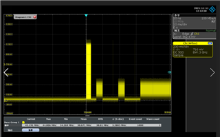
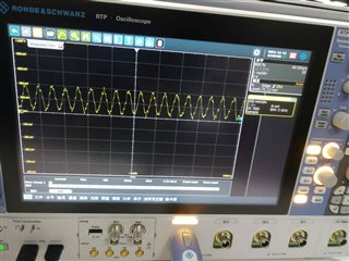
The DDR clk we measured with the oscilloscope seems to be normal.

Could give me some suggestion about this issue?

Best Regards

Nathan

  • Fix:Timeout during frequency hands -> Timeout during frequency handshake

  • Hi Nathan,

    Can you comment on whether this is a TI EVM, or your custom board? The error message indicates that the DDR training did not complete. 

    Can you try the changes below and see if this has any impact?

    Thanks,
    Kevin

    • For below registers, change the '7' to a '6' as shown below

    #define DDRSS_PHY_33_DATA 0x0C002006
    #define DDRSS_PHY_289_DATA 0x0C002006
    #define DDRSS_PHY_545_DATA 0x0C002006
    #define DDRSS_PHY_801_DATA 0x0C002006

    • For below registers, change the '20' to a '40' as shown below

    #define DDRSS_PHY_32_DATA 0x10400000
    #define DDRSS_PHY_288_DATA 0x10400000
    #define DDRSS_PHY_544_DATA 0x10400000
    #define DDRSS_PHY_800_DATA 0x10400000

  • Hi Kevin,

    Thanks for your reply!

    This is our custom board.

    I would try your patch.

    Best Regards

    Nathan

  • Hi Kevin,

    I have tried your patch and it does not work.

    The uart log is:

    U-Boot SPL 2020.01 (Nov 15 2021 - 16:33:17 +0800)
    SYSFW ABI: 3.0 (firmware rev 0x0014 '20.04.1-v2020.04a (Terrific Lla')
    Reading on-board EEPROM at 0x50 failed 1
    j721e_ddrss_probe(dev=41c87a60)
    j721e_ddrss_ofdata_to_priv(dev=41c87a60)
    j721e_ddrss_power_on(ddrss=41ccc004)
    LPDDR4_Probe: PASS
    LPDDR4_Init: PASS
    --->>> LPDDR4 Initialization is in progress ... <<<---
    j721e_lpddr4_ack_freq_upd_req: received freq change req: req type = 1, req no. = 0
    j721e_lpddr4_ack_freq_upd_req: received freq change req: req type = 0, req no. = 1
    j721e_lpddr4_ack_freq_upd_req: received freq change req: req type = 1, req no. = 2
    j721e_lpddr4_ack_freq_upd_req: received freq change req: req type = 0, req no. = 3
    j721e_lpddr4_ack_freq_upd_req: received freq change req: req type = 1, req no. = 4
    wait_for_bit_le32: Timeout (reg=114080 mask=80 wait_set=)
    Timeout during frequency handshake
    ### ERROR ### Please RESET the board ###

    Best Regards

    Nathan

  • Hi Nathan,

    Thanks for the update, can you also let us know what memory you are using? Since this is a custom board, have you already filled out the Register Configuration tool and updated the settings in u-boot? 

    You can access the register configuration tool here: https://www.ti.com/lit/pdf/spracu8

    Regards,
    Kevin

  • Hi, Kevin

    The memory is MT53D1024M32D4DT-046 AAT:D, and we already filled out the Register Configuration tool and updated the settings in u-boot.

    Best Regards

    Nathan

  • Hi, Kevin,

    About this problem, do you have any other ideas?

    Best Regards

    Nathan

  • Hi Nathan,

    I have sent my colleague a binary file to run on the R5 (loaded through CCS / JTAG) that will capture additional helpful information. Can you please collect this data by using this binary when the issue occurs, and send the data back to my colleague? Can you also please provide the filled in XLS sheet?

    Thanks,
    Kevin 

  • Hi, Kevin,

    Thanks for your reply!

    I tried to load this binary, but I don't see any output.What is the data you are talking about?


    The xls file is Jacinto7_DDRSS_RegConfigTool_micron3733.xlsm and we change the values of DDRSS PHY 33,289,801 from 0x0C002007 to 0x0C002006.

    Best Regards

    Nathan

  • Hi Nathan,

    If you haven't already, can you try re-setting the R5 core (software reset) through CCS before loading the code? The output should appear on the CCS console window.

    Also, can you provide the following information:

    • How many boards does this issue occur on? (both raw count and percentage, ex: "5 out of 10 boards")
    • Does the issue also occur if you reduce the DDR frequency to something slower? (ex: 2133 MHz data rate)

    Regards,
    Kevin

  • Hi Kevin,

    The attachment is the output of the ccs console.

    [MCU_Cortex_R5_0] Training Results; Frequency 0; CS 0
    PHY Vref Training:
    	 DQ Lane 0 Vref Mode: 0x7 Vref Sel: 0x23
    	 DQ Lane 1 Vref Mode: 0x7 Vref Sel: 0x24
    	 DQ Lane 2 Vref Mode: 0x7 Vref Sel: 0x1b
    	 DQ Lane 3 Vref Mode: 0x7 Vref Sel: 0x26
    	 ACC Vref Control: 0x7ab 
    CA Training:
    	 LP4 CA Programmed Delays:
    	 CA Bit 0 delay: 37e 
    	 CA Bit 1 delay: 320 
    	 CA Bit 2 delay: 380 
    	 CA Bit 3 delay: 33c 
    	 CA Bit 4 delay: 376 
    	 CA Bit 5 delay: 346 
    Write Leveling:
    	 DQ Lane 0 WRDQS: 0xba 
    	 DQ Lane 1 WRDQS: 0x9c 
    	 DQ Lane 2 WRDQS: 0xd2 
    	 DQ Lane 3 WRDQS: 0xba 
    	 DQ Lane 0 Write Path Latency Add: 0x0 
    	 DQ Lane 1 Write Path Latency Add: 0x0 
    	 DQ Lane 2 Write Path Latency Add: 0x0 
    	 DQ Lane 3 Write Path Latency Add: 0x0 
    Gate Training: 
    	 DQS Gate Lane 0 : slave_delay: 328 lat_adj: 5
    	 DQS Gate Lane 1 : slave_delay: 340 lat_adj: 5
    	 DQS Gate Lane 2 : slave_delay: 304 lat_adj: 5
    	 DQS Gate Lane 3 : slave_delay: 340 lat_adj: 5
    Read Leveling:
    	read_delay_fall, dq0 : 150
    	read_delay_rise, dq0 : 162
    	read_delay_fall, dq1 : 162
    	read_delay_rise, dq1 : 162
    	read_delay_fall, dq2 : 150
    	read_delay_rise, dq2 : 162
    	read_delay_fall, dq3 : 168
    	read_delay_rise, dq3 : 174
    	read_delay_fall, dq4 : 150
    	read_delay_rise, dq4 : 150
    	read_delay_fall, dq5 : 162
    	read_delay_rise, dq5 : 150
    	read_delay_fall, dq6 : 144
    	read_delay_rise, dq6 : 150
    	read_delay_fall, dq7 : 162
    	read_delay_rise, dq7 : 162
    	read_delay_fall, dq8 : 180
    	read_delay_rise, dq8 : 168
    	read_delay_fall, dq9 : 174
    	read_delay_rise, dq9 : 168
    	read_delay_fall, dq10 : 168
    	read_delay_rise, dq10 : 168
    	read_delay_fall, dq11 : 174
    	read_delay_rise, dq11 : 174
    	read_delay_fall, dq12 : 162
    	read_delay_rise, dq12 : 156
    	read_delay_fall, dq13 : 168
    	read_delay_rise, dq13 : 168
    	read_delay_fall, dq14 : 156
    	read_delay_rise, dq14 : 144
    	read_delay_fall, dq15 : 174
    	read_delay_rise, dq15 : 168
    	read_delay_fall, dq16 : 733
    	read_delay_rise, dq16 : 150
    	read_delay_fall, dq17 : 733
    	read_delay_rise, dq17 : 150
    	read_delay_fall, dq18 : 733
    	read_delay_rise, dq18 : 150
    	read_delay_fall, dq19 : 733
    	read_delay_rise, dq19 : 156
    	read_delay_fall, dq20 : 733
    	read_delay_rise, dq20 : 150
    	read_delay_fall, dq21 : 733
    	read_delay_rise, dq21 : 144
    	read_delay_fall, dq22 : 733
    	read_delay_rise, dq22 : 138
    	read_delay_fall, dq23 : 733
    	read_delay_rise, dq23 : 156
    	read_delay_fall, dq24 : 168
    	read_delay_rise, dq24 : 156
    	read_delay_fall, dq25 : 162
    	read_delay_rise, dq25 : 156
    	read_delay_fall, dq26 : 174
    	read_delay_rise, dq26 : 156
    	read_delay_fall, dq27 : 174
    	read_delay_rise, dq27 : 162
    	read_delay_fall, dq28 : 162
    	read_delay_rise, dq28 : 150
    	read_delay_fall, dq29 : 174
    	read_delay_rise, dq29 : 156
    	read_delay_fall, dq30 : 162
    	read_delay_rise, dq30 : 144
    	read_delay_fall, dq31 : 174
    	read_delay_rise, dq31 : 162
    Write DQ Training:
    	write_delay, dq0 : 640
    	write_delay, dq1 : 640
    	write_delay, dq2 : 640
    	write_delay, dq3 : 640
    	write_delay, dq4 : 640
    	write_delay, dq5 : 640
    	write_delay, dq6 : 640
    	write_delay, dq7 : 640
    	write_delay, dq8 : 640
    	write_delay, dq9 : 640
    	write_delay, dq10 : 640
    	write_delay, dq11 : 640
    	write_delay, dq12 : 640
    	write_delay, dq13 : 640
    	write_delay, dq14 : 640
    	write_delay, dq15 : 640
    	write_delay, dq16 : 640
    	write_delay, dq17 : 640
    	write_delay, dq18 : 640
    	write_delay, dq19 : 640
    	write_delay, dq20 : 640
    	write_delay, dq21 : 640
    	write_delay, dq22 : 640
    	write_delay, dq23 : 640
    	write_delay, dq24 : 640
    	write_delay, dq25 : 640
    	write_delay, dq26 : 640
    	write_delay, dq27 : 640
    	write_delay, dq28 : 640
    	write_delay, dq29 : 640
    	write_delay, dq30 : 640
    	write_delay, dq31 : 640
    Calibration Registers:
    	CAL_OBS_0: 0x00812654
    	CAL_OBS_2: 0x00812792
    	CAL_OBS_3: 0xb3000000
    	CAL_OBS_4: 0x00126544
    	CAL_OBS_5: 0x00127928
    	CAL_OBS_6: 0x00f2654f
    	CAL_OBS_7: 0x03f2792f
    CS Programmed Delays:
    	phy_grp0_slave_delay_0: 0x034c
    	phy_grp1_slave_delay_0: 0x034c
    	phy_grp2_slave_delay_0: 0x0350
    	phy_grp3_slave_delay_0: 0x035e
    	phy_grp0_slave_delay_1: 0x0356
    	phy_grp1_slave_delay_1: 0x034c
    	phy_grp2_slave_delay_1: 0x0350
    	phy_grp3_slave_delay_1: 0x0356
    	phy_top_train_calib_error_info: 0x00000000
    Training Results; Frequency 0; CS 1
    PHY Vref Training:
    	 DQ Lane 0 Vref Mode: 0x7 Vref Sel: 0x23
    	 DQ Lane 1 Vref Mode: 0x7 Vref Sel: 0x24
    	 DQ Lane 2 Vref Mode: 0x7 Vref Sel: 0x1b
    	 DQ Lane 3 Vref Mode: 0x7 Vref Sel: 0x26
    	 ACC Vref Control: 0x7ab 
    CA Training:
    	 LP4 CA Programmed Delays:
    	 CA Bit 0 delay: 37e 
    	 CA Bit 1 delay: 320 
    	 CA Bit 2 delay: 380 
    	 CA Bit 3 delay: 33c 
    	 CA Bit 4 delay: 376 
    	 CA Bit 5 delay: 346 
    Write Leveling:
    	 DQ Lane 0 WRDQS: 0xb4 
    	 DQ Lane 1 WRDQS: 0x96 
    	 DQ Lane 2 WRDQS: 0xcc 
    	 DQ Lane 3 WRDQS: 0xa2 
    	 DQ Lane 0 Write Path Latency Add: 0x0 
    	 DQ Lane 1 Write Path Latency Add: 0x0 
    	 DQ Lane 2 Write Path Latency Add: 0x0 
    	 DQ Lane 3 Write Path Latency Add: 0x0 
    Gate Training: 
    	 DQS Gate Lane 0 : slave_delay: 478 lat_adj: 5
    	 DQS Gate Lane 1 : slave_delay: 490 lat_adj: 5
    	 DQS Gate Lane 2 : slave_delay: 406 lat_adj: 5
    	 DQS Gate Lane 3 : slave_delay: 454 lat_adj: 5
    Read Leveling:
    	read_delay_fall, dq0 : 160
    	read_delay_rise, dq0 : 160
    	read_delay_fall, dq1 : 160
    	read_delay_rise, dq1 : 160
    	read_delay_fall, dq2 : 160
    	read_delay_rise, dq2 : 160
    	read_delay_fall, dq3 : 160
    	read_delay_rise, dq3 : 160
    	read_delay_fall, dq4 : 160
    	read_delay_rise, dq4 : 160
    	read_delay_fall, dq5 : 160
    	read_delay_rise, dq5 : 160
    	read_delay_fall, dq6 : 160
    	read_delay_rise, dq6 : 160
    	read_delay_fall, dq7 : 160
    	read_delay_rise, dq7 : 160
    	read_delay_fall, dq8 : 160
    	read_delay_rise, dq8 : 160
    	read_delay_fall, dq9 : 160
    	read_delay_rise, dq9 : 160
    	read_delay_fall, dq10 : 160
    	read_delay_rise, dq10 : 160
    	read_delay_fall, dq11 : 160
    	read_delay_rise, dq11 : 160
    	read_delay_fall, dq12 : 160
    	read_delay_rise, dq12 : 160
    	read_delay_fall, dq13 : 160
    	read_delay_rise, dq13 : 160
    	read_delay_fall, dq14 : 160
    	read_delay_rise, dq14 : 160
    	read_delay_fall, dq15 : 160
    	read_delay_rise, dq15 : 160
    	read_delay_fall, dq16 : 160
    	read_delay_rise, dq16 : 160
    	read_delay_fall, dq17 : 160
    	read_delay_rise, dq17 : 160
    	read_delay_fall, dq18 : 160
    	read_delay_rise, dq18 : 160
    	read_delay_fall, dq19 : 160
    	read_delay_rise, dq19 : 160
    	read_delay_fall, dq20 : 160
    	read_delay_rise, dq20 : 160
    	read_delay_fall, dq21 : 160
    	read_delay_rise, dq21 : 160
    	read_delay_fall, dq22 : 160
    	read_delay_rise, dq22 : 160
    	read_delay_fall, dq23 : 160
    	read_delay_rise, dq23 : 160
    	read_delay_fall, dq24 : 160
    	read_delay_rise, dq24 : 160
    	read_delay_fall, dq25 : 160
    	read_delay_rise, dq25 : 160
    	read_delay_fall, dq26 : 160
    	read_delay_rise, dq26 : 160
    	read_delay_fall, dq27 : 160
    	read_delay_rise, dq27 : 160
    	read_delay_fall, dq28 : 160
    	read_delay_rise, dq28 : 160
    	read_delay_fall, dq29 : 160
    	read_delay_rise, dq29 : 160
    	read_delay_fall, dq30 : 160
    	read_delay_rise, dq30 : 160
    	read_delay_fall, dq31 : 160
    	read_delay_rise, dq31 : 160
    Write DQ Training:
    	write_delay, dq0 : 640
    	write_delay, dq1 : 640
    	write_delay, dq2 : 640
    	write_delay, dq3 : 640
    	write_delay, dq4 : 640
    	write_delay, dq5 : 640
    	write_delay, dq6 : 640
    	write_delay, dq7 : 640
    	write_delay, dq8 : 640
    	write_delay, dq9 : 640
    	write_delay, dq10 : 640
    	write_delay, dq11 : 640
    	write_delay, dq12 : 640
    	write_delay, dq13 : 640
    	write_delay, dq14 : 640
    	write_delay, dq15 : 640
    	write_delay, dq16 : 640
    	write_delay, dq17 : 640
    	write_delay, dq18 : 640
    	write_delay, dq19 : 640
    	write_delay, dq20 : 640
    	write_delay, dq21 : 640
    	write_delay, dq22 : 640
    	write_delay, dq23 : 640
    	write_delay, dq24 : 640
    	write_delay, dq25 : 640
    	write_delay, dq26 : 640
    	write_delay, dq27 : 640
    	write_delay, dq28 : 640
    	write_delay, dq29 : 640
    	write_delay, dq30 : 640
    	write_delay, dq31 : 640
    Calibration Registers:
    	CAL_OBS_0: 0x00812654
    	CAL_OBS_2: 0x00812792
    	CAL_OBS_3: 0xb3000000
    	CAL_OBS_4: 0x00126544
    	CAL_OBS_5: 0x00127928
    	CAL_OBS_6: 0x00f2654f
    	CAL_OBS_7: 0x03f2792f
    CS Programmed Delays:
    	phy_grp0_slave_delay_0: 0x034c
    	phy_grp1_slave_delay_0: 0x034c
    	phy_grp2_slave_delay_0: 0x0350
    	phy_grp3_slave_delay_0: 0x035e
    	phy_grp0_slave_delay_1: 0x0356
    	phy_grp1_slave_delay_1: 0x034c
    	phy_grp2_slave_delay_1: 0x0350
    	phy_grp3_slave_delay_1: 0x0356
    	phy_top_train_calib_error_info: 0x00000000
    Training Results; Frequency 1; CS 0
    PHY Vref Training:
    	 DQ Lane 0 Vref Mode: 0x7 Vref Sel: 0x2b
    	 DQ Lane 1 Vref Mode: 0x7 Vref Sel: 0x2b
    	 DQ Lane 2 Vref Mode: 0x7 Vref Sel: 0x2b
    	 DQ Lane 3 Vref Mode: 0x7 Vref Sel: 0x2b
    	 ACC Vref Control: 0x7ab 
    CA Training:
    	 LP4 CA Programmed Delays:
    	 CA Bit 0 delay: 300 
    	 CA Bit 1 delay: 300 
    	 CA Bit 2 delay: 300 
    	 CA Bit 3 delay: 300 
    	 CA Bit 4 delay: 300 
    	 CA Bit 5 delay: 300 
    Write Leveling:
    	 DQ Lane 0 WRDQS: 0x0 
    	 DQ Lane 1 WRDQS: 0x0 
    	 DQ Lane 2 WRDQS: 0x0 
    	 DQ Lane 3 WRDQS: 0x0 
    	 DQ Lane 0 Write Path Latency Add: 0x0 
    	 DQ Lane 1 Write Path Latency Add: 0x0 
    	 DQ Lane 2 Write Path Latency Add: 0x0 
    	 DQ Lane 3 Write Path Latency Add: 0x0 
    Gate Training: 
    	 DQS Gate Lane 0 : slave_delay: 109 lat_adj: 5
    	 DQS Gate Lane 1 : slave_delay: 109 lat_adj: 5
    	 DQS Gate Lane 2 : slave_delay: 109 lat_adj: 5
    	 DQS Gate Lane 3 : slave_delay: 109 lat_adj: 5
    Read Leveling:
    	read_delay_fall, dq0 : 160
    	read_delay_rise, dq0 : 160
    	read_delay_fall, dq1 : 160
    	read_delay_rise, dq1 : 160
    	read_delay_fall, dq2 : 160
    	read_delay_rise, dq2 : 160
    	read_delay_fall, dq3 : 160
    	read_delay_rise, dq3 : 160
    	read_delay_fall, dq4 : 160
    	read_delay_rise, dq4 : 160
    	read_delay_fall, dq5 : 160
    	read_delay_rise, dq5 : 160
    	read_delay_fall, dq6 : 160
    	read_delay_rise, dq6 : 160
    	read_delay_fall, dq7 : 160
    	read_delay_rise, dq7 : 160
    	read_delay_fall, dq8 : 160
    	read_delay_rise, dq8 : 160
    	read_delay_fall, dq9 : 160
    	read_delay_rise, dq9 : 160
    	read_delay_fall, dq10 : 160
    	read_delay_rise, dq10 : 160
    	read_delay_fall, dq11 : 160
    	read_delay_rise, dq11 : 160
    	read_delay_fall, dq12 : 160
    	read_delay_rise, dq12 : 160
    	read_delay_fall, dq13 : 160
    	read_delay_rise, dq13 : 160
    	read_delay_fall, dq14 : 160
    	read_delay_rise, dq14 : 160
    	read_delay_fall, dq15 : 160
    	read_delay_rise, dq15 : 160
    	read_delay_fall, dq16 : 160
    	read_delay_rise, dq16 : 160
    	read_delay_fall, dq17 : 160
    	read_delay_rise, dq17 : 160
    	read_delay_fall, dq18 : 160
    	read_delay_rise, dq18 : 160
    	read_delay_fall, dq19 : 160
    	read_delay_rise, dq19 : 160
    	read_delay_fall, dq20 : 160
    	read_delay_rise, dq20 : 160
    	read_delay_fall, dq21 : 160
    	read_delay_rise, dq21 : 160
    	read_delay_fall, dq22 : 160
    	read_delay_rise, dq22 : 160
    	read_delay_fall, dq23 : 160
    	read_delay_rise, dq23 : 160
    	read_delay_fall, dq24 : 160
    	read_delay_rise, dq24 : 160
    	read_delay_fall, dq25 : 160
    	read_delay_rise, dq25 : 160
    	read_delay_fall, dq26 : 160
    	read_delay_rise, dq26 : 160
    	read_delay_fall, dq27 : 160
    	read_delay_rise, dq27 : 160
    	read_delay_fall, dq28 : 160
    	read_delay_rise, dq28 : 160
    	read_delay_fall, dq29 : 160
    	read_delay_rise, dq29 : 160
    	read_delay_fall, dq30 : 160
    	read_delay_rise, dq30 : 160
    	read_delay_fall, dq31 : 160
    	read_delay_rise, dq31 : 160
    Write DQ Training:
    	write_delay, dq0 : 640
    	write_delay, dq1 : 640
    	write_delay, dq2 : 640
    	write_delay, dq3 : 640
    	write_delay, dq4 : 640
    	write_delay, dq5 : 640
    	write_delay, dq6 : 640
    	write_delay, dq7 : 640
    	write_delay, dq8 : 640
    	write_delay, dq9 : 640
    	write_delay, dq10 : 640
    	write_delay, dq11 : 640
    	write_delay, dq12 : 640
    	write_delay, dq13 : 640
    	write_delay, dq14 : 640
    	write_delay, dq15 : 640
    	write_delay, dq16 : 640
    	write_delay, dq17 : 640
    	write_delay, dq18 : 640
    	write_delay, dq19 : 640
    	write_delay, dq20 : 640
    	write_delay, dq21 : 640
    	write_delay, dq22 : 640
    	write_delay, dq23 : 640
    	write_delay, dq24 : 640
    	write_delay, dq25 : 640
    	write_delay, dq26 : 640
    	write_delay, dq27 : 640
    	write_delay, dq28 : 640
    	write_delay, dq29 : 640
    	write_delay, dq30 : 640
    	write_delay, dq31 : 640
    Calibration Registers:
    	CAL_OBS_0: 0x00812654
    	CAL_OBS_2: 0x00812792
    	CAL_OBS_3: 0xb3000000
    	CAL_OBS_4: 0x00126544
    	CAL_OBS_5: 0x00127928
    	CAL_OBS_6: 0x00f2654f
    	CAL_OBS_7: 0x03f2792f
    CS Programmed Delays:
    	phy_grp0_slave_delay_0: 0x0390
    	phy_grp1_slave_delay_0: 0x0390
    	phy_grp2_slave_delay_0: 0x0390
    	phy_grp3_slave_delay_0: 0x0390
    	phy_grp0_slave_delay_1: 0x0390
    	phy_grp1_slave_delay_1: 0x0390
    	phy_grp2_slave_delay_1: 0x0390
    	phy_grp3_slave_delay_1: 0x0390
    	phy_top_train_calib_error_info: 0x00000000
    Training Results; Frequency 1; CS 1
    PHY Vref Training:
    	 DQ Lane 0 Vref Mode: 0x7 Vref Sel: 0x2b
    	 DQ Lane 1 Vref Mode: 0x7 Vref Sel: 0x2b
    	 DQ Lane 2 Vref Mode: 0x7 Vref Sel: 0x2b
    	 DQ Lane 3 Vref Mode: 0x7 Vref Sel: 0x2b
    	 ACC Vref Control: 0x7ab 
    CA Training:
    	 LP4 CA Programmed Delays:
    	 CA Bit 0 delay: 300 
    	 CA Bit 1 delay: 300 
    	 CA Bit 2 delay: 300 
    	 CA Bit 3 delay: 300 
    	 CA Bit 4 delay: 300 
    	 CA Bit 5 delay: 300 
    Write Leveling:
    	 DQ Lane 0 WRDQS: 0x0 
    	 DQ Lane 1 WRDQS: 0x0 
    	 DQ Lane 2 WRDQS: 0x0 
    	 DQ Lane 3 WRDQS: 0x0 
    	 DQ Lane 0 Write Path Latency Add: 0x0 
    	 DQ Lane 1 Write Path Latency Add: 0x0 
    	 DQ Lane 2 Write Path Latency Add: 0x0 
    	 DQ Lane 3 Write Path Latency Add: 0x0 
    Gate Training: 
    	 DQS Gate Lane 0 : slave_delay: 109 lat_adj: 5
    	 DQS Gate Lane 1 : slave_delay: 109 lat_adj: 5
    	 DQS Gate Lane 2 : slave_delay: 109 lat_adj: 5
    	 DQS Gate Lane 3 : slave_delay: 109 lat_adj: 5
    Read Leveling:
    	read_delay_fall, dq0 : 160
    	read_delay_rise, dq0 : 160
    	read_delay_fall, dq1 : 160
    	read_delay_rise, dq1 : 160
    	read_delay_fall, dq2 : 160
    	read_delay_rise, dq2 : 160
    	read_delay_fall, dq3 : 160
    	read_delay_rise, dq3 : 160
    	read_delay_fall, dq4 : 160
    	read_delay_rise, dq4 : 160
    	read_delay_fall, dq5 : 160
    	read_delay_rise, dq5 : 160
    	read_delay_fall, dq6 : 160
    	read_delay_rise, dq6 : 160
    	read_delay_fall, dq7 : 160
    	read_delay_rise, dq7 : 160
    	read_delay_fall, dq8 : 160
    	read_delay_rise, dq8 : 160
    	read_delay_fall, dq9 : 160
    	read_delay_rise, dq9 : 160
    	read_delay_fall, dq10 : 160
    	read_delay_rise, dq10 : 160
    	read_delay_fall, dq11 : 160
    	read_delay_rise, dq11 : 160
    	read_delay_fall, dq12 : 160
    	read_delay_rise, dq12 : 160
    	read_delay_fall, dq13 : 160
    	read_delay_rise, dq13 : 160
    	read_delay_fall, dq14 : 160
    	read_delay_rise, dq14 : 160
    	read_delay_fall, dq15 : 160
    	read_delay_rise, dq15 : 160
    	read_delay_fall, dq16 : 160
    	read_delay_rise, dq16 : 160
    	read_delay_fall, dq17 : 160
    	read_delay_rise, dq17 : 160
    	read_delay_fall, dq18 : 160
    	read_delay_rise, dq18 : 160
    	read_delay_fall, dq19 : 160
    	read_delay_rise, dq19 : 160
    	read_delay_fall, dq20 : 160
    	read_delay_rise, dq20 : 160
    	read_delay_fall, dq21 : 160
    	read_delay_rise, dq21 : 160
    	read_delay_fall, dq22 : 160
    	read_delay_rise, dq22 : 160
    	read_delay_fall, dq23 : 160
    	read_delay_rise, dq23 : 160
    	read_delay_fall, dq24 : 160
    	read_delay_rise, dq24 : 160
    	read_delay_fall, dq25 : 160
    	read_delay_rise, dq25 : 160
    	read_delay_fall, dq26 : 160
    	read_delay_rise, dq26 : 160
    	read_delay_fall, dq27 : 160
    	read_delay_rise, dq27 : 160
    	read_delay_fall, dq28 : 160
    	read_delay_rise, dq28 : 160
    	read_delay_fall, dq29 : 160
    	read_delay_rise, dq29 : 160
    	read_delay_fall, dq30 : 160
    	read_delay_rise, dq30 : 160
    	read_delay_fall, dq31 : 160
    	read_delay_rise, dq31 : 160
    Write DQ Training:
    	write_delay, dq0 : 640
    	write_delay, dq1 : 640
    	write_delay, dq2 : 640
    	write_delay, dq3 : 640
    	write_delay, dq4 : 640
    	write_delay, dq5 : 640
    	write_delay, dq6 : 640
    	write_delay, dq7 : 640
    	write_delay, dq8 : 640
    	write_delay, dq9 : 640
    	write_delay, dq10 : 640
    	write_delay, dq11 : 640
    	write_delay, dq12 : 640
    	write_delay, dq13 : 640
    	write_delay, dq14 : 640
    	write_delay, dq15 : 640
    	write_delay, dq16 : 640
    	write_delay, dq17 : 640
    	write_delay, dq18 : 640
    	write_delay, dq19 : 640
    	write_delay, dq20 : 640
    	write_delay, dq21 : 640
    	write_delay, dq22 : 640
    	write_delay, dq23 : 640
    	write_delay, dq24 : 640
    	write_delay, dq25 : 640
    	write_delay, dq26 : 640
    	write_delay, dq27 : 640
    	write_delay, dq28 : 640
    	write_delay, dq29 : 640
    	write_delay, dq30 : 640
    	write_delay, dq31 : 640
    Calibration Registers:
    	CAL_OBS_0: 0x00812654
    	CAL_OBS_2: 0x00812792
    	CAL_OBS_3: 0xb3000000
    	CAL_OBS_4: 0x00126544
    	CAL_OBS_5: 0x00127928
    	CAL_OBS_6: 0x00f2654f
    	CAL_OBS_7: 0x03f2792f
    CS Programmed Delays:
    	phy_grp0_slave_delay_0: 0x0390
    	phy_grp1_slave_delay_0: 0x0390
    	phy_grp2_slave_delay_0: 0x0390
    	phy_grp3_slave_delay_0: 0x0390
    	phy_grp0_slave_delay_1: 0x0390
    	phy_grp1_slave_delay_1: 0x0390
    	phy_grp2_slave_delay_1: 0x0390
    	phy_grp3_slave_delay_1: 0x0390
    	phy_top_train_calib_error_info: 0x00000000
    DRAM VREF Values:
    	mr12_f1_cs0: 0x00000016
    	mr12_f1_cs1: 0x00000016
    	mr12_f1_cs2: 0x00000016
    	mr12_f1_cs3: 0x00000017
    	mr12_f2_cs0: 0x00000027
    	mr12_f2_cs1: 0x00000027
    	mr12_f2_cs2: 0x00000027
    	mr12_f2_cs3: 0x00000027
    	mr14_f1_cs0: 0x0000000f
    	mr14_f1_cs1: 0x0000000f
    	mr14_f1_cs2: 0x0000000f
    	mr14_f1_cs3: 0x0000000f
    	mr14_f2_cs0: 0x0000000f
    	mr14_f2_cs1: 0x0000000f
    	mr14_f2_cs2: 0x0000000f
    	mr14_f2_cs3: 0x0000000f
    PHY IO Pad TERM Registers:
    	PHY_1320: 0x00012654
    	PHY_1321: 0x00012654
    	PHY_1322: 0x00012654
    	PHY_1323: 0x00012654
    	PHY_1324: 0x00012654
    	PHY_1325: 0x00012792
    	PHY_1326: 0x00012792
    	PHY_1327: 0x00012654
    	PHY_1328: 0x00012654
    Enhanced Error Reporting:
    	DQS Gate Error: 0 
    	Training Error: 0 
    	FSM Tran Error: 0 
    	PLL      Error: 0 
    	Parity   Error: 0 
    	Timeout  Error: 1 
    	Timeout Error Info: 
    		dfi_rddata_valid           Timeout: 0 
    		Max PLL lock assertion     Timeout: 1 
    		Min PLL lock assertion     Timeout: 0 
    		DFI PHY master interface   Timeout: 0 
    		dfi_phyupd_req (PI - PHY)  Timeout: 0 
    		dfi_phyupd_req (CTL - PHY) Timeout: 0 
    		dfi_lp_ack                 Timeout: 0 
    		DFS change @ PI - PHY      Timeout: 0 
    		DFS change @ CTL -PHY      Timeout: 1 
    		CA / CS training           Timeout: 0 
    		WRLVL training             Timeout: 0 
    		RDGATE training            Timeout: 0 
    		RDDATA training            Timeout: 1 
    		WDQ training               Timeout: 0 


    The number of the board is about 2 out of 300.

    I tried reduse the DDR frequency from 1866 MHz to 1200 MHz and it not work.

    Best Regards

    Nathan

  • Hi Nathan,

    Thanks, it looks like the READ DQ training on byte lane 2 failed. 

    Can you confirm that on the 2 boards (of 300) which show the issue, does the issue occur 100% of the time, or just occasionally? 

    Also, you mentioned that you were using SDK7.3. Do you see the same issue on these 2 boards if you were to switch to SDK7.2?

    Thanks,
    Kevin

  • Hi Kevin,

    Thanks and the issue occured 100% of the time.

    Sorry, I have not tried to switch to SDK7.2 and what about the difference between the SDK7.2 and SDK7.3?

    Best Regards

    Nathan