This thread has been locked.

If you have a related question, please click the "Ask a related question" button in the top right corner. The newly created question will be automatically linked to this question.

TMS320C6748: Inquiry about “2.1.4 System-Level ESD Immunity Usage Note” in errata document

Part Number: TMS320C6748
Other Parts Discussed in Thread: TMDSLCDK6748,

Hi Team,

Our customer is developing their system with TMS320C6748EZWT4. Customer was evaluating the Noise Immunity test with their system, they encountered the issue which their system freeze suddenly. Customer noticed there are descriptions about ESD Immunity in C6748 Errata (https://www.ti.com/lit/pdf/sprz303 : 2.1.4 System-Level ESD Immunity Usage Note). Since customer would like to understand it exactly, we received some inquires about this  2.1.4 section, as follows.

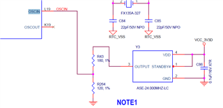
  1. Regarding “Figure 2. External 3.3V Clock Source”,  customer understands X1 means an external oscillator. Is customer’s understanding correct?
  2. If so, customer wants to know what OSCOUT means. Does this mean the clock-out pin?
  3. For the oscillator which customer used, Customer mentioned there is not VDD, GND and Enable-pin.  Customer would like to clarify this X1 device.

I believe customer is using the crystal (not oscillator). Since TI recommends external oscillator implementation for ESD robustness, I suppose we should share the information about the oscillator which TI recommends. Can I have your Expert’s advice/comments on this, please?

As far as I checked TMDSLCDK6748 -EVM’s schematic ( https://www.ti.com/lit/zip/sprcaf4 ), I believe the above implementation is accomplished in our EVM. Should I request customer to refer this schematic? And can I mention TI recommends ASE-24.000MHZ-LC?

Best regards,

Miyazaki

  • 1. Yes, X1 is an LVCMOS oscillator with its output level shifted down with a voltage divider, as shown in Figure 2.  The divider reduces the 3.3v swing down to the appropriate voltage swing defined for the OSCIN pin. We recommend selecting an LVCMOS clock source that has a maximum output rise/fall times less than 5ns. Note: Many oscillator datasheets define rise/fall time with maximum load capacitance, which will slow the rise/fall. However, the rise/fall is very likely to be much faster in this use case since the capacitive load is very small. So there is a good chance most oscillators will have output rise/fall times faster than 5ns. However, your customer would need to confirm this with the oscillator manufacture or verify it themselves.

    2. Yes, it is pin K19.

    3. It sounds like the customer used a crystal rather than an LVCMOS oscillator. It doesn't sound like they read the errata before designing their board and missed the advisory warning this issue. They need to redesign their board to use an LVCMOS oscillator as the reference clock source for TMS320C6748.

    Regards,
    Paul 

  • Hi Paul,

    Thank you for your  clarification and advice.

    I shared your comments with customer. I'd like to wait customer's feedback for a while.

    Best regards,

    Miyazaki