This thread has been locked.

If you have a related question, please click the "Ask a related question" button in the top right corner. The newly created question will be automatically linked to this question.

TMS320C6747: McAsp0 and Emac ports usage at the same time

Part Number: TMS320C6747

Sir/Madam,

I am developing a board based on c6747 DSP. My application requires interface to 4 codec ICs AIC3106,  4 ADC6140 ICs and EMAC port. 

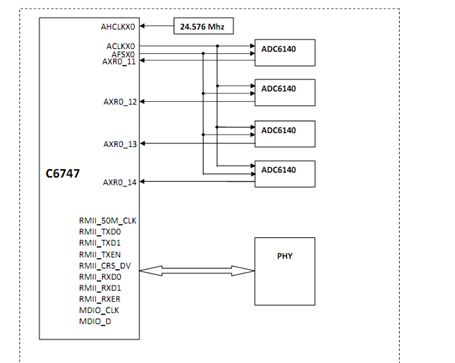
I am planning to use

1.  Four Codec ICs by interfacing them with McAsp1

2.  Four ADC6140 ICs by interfacing them with McAsp0 (AHCLKX0, ACLKX0, AFSX0 and 4 serializers AXR11 to AXR14).

3. Use EMAC port to connect it to a PHY. (Please refer interface diagram Mcasp0 and EMAC).

/resized-image/__size/455x364/__key/communityserver-discussions-components-files/791/pastedimage1638347562417v2.png


I have developed a similar board in my previous project which is  working fine. Only difference in that board is that there was no ethernet in it

and I had used McAsp1 port for 4 codec ICs, Mcap0 port (AHCLKR0, ACLKR0, AFSR0 and 4 serializers AXR0 to AXR3) with ADC6140 ICs.

Now Please clarify following.

1. Can I use AHCLKX0, ACLKX0, AFSX0 pins to interface with ADC6140 instead of AHCLKR0, ACLKR0, AFSR0 as I can not use AHCLKR0 pin because it is multiplexed with RMII_50M_CLK.

2. Can I use EMAC and Mcasp0 at the same time by configuring AHCLKX0, ACLKX0, AFSX0,AXR11 to AXR14 pins as Mcasp0 and remaining pins as EMAC.

regards

Jagdish Patange

SLRDC, HAL Hyderabad

  • Hi Jagdish,

    1. Can I use AHCLKX0, ACLKX0, AFSX0 pins to interface with ADC6140 instead of AHCLKR0, ACLKR0, AFSR0 as I can not use AHCLKR0 pin because it is multiplexed with RMII_50M_CLK.

    Yes. McASP receiver can be clocked with the transmitter clock and frame sync.
    But you may not need to do this since AHCLKR0 may not be required if you generate the bit clock and frame sync from one of the ADC6140s.

    See C6747 TRM SPRUH91D
    24.0.21.1.5 Synchronous Transmit and Receive Operation (ASYNC = 0)
    24.1.29 Transmit Clock Control Register (ACLKXCTL)

    ACLKXCTL[6] ASYNC
    Transmit/receive operation asynchronous enable bit.
     * 0 = Synchronous. Transmit clock and frame sync provides the source for both the transmit and receive sections. Note that in this mode, the receive bit clock is an inverted version of the transmit bit clock. See Section 24.0.21.1.5 for more details.
     * 1 = Asynchronous. Separate clock and frame sync used by transmit and receive sections.

    Checking the ADC6140 datasheet...It appears it can generate the clocks, and there is this note that states the BCLK output clock frequency must be lower than 18.5 MHz (to meet the timing specifications), if the SDOUT data line is latched on the opposite BCLK edge polarity than the edge used by the device to transmit SDOUT data.

    See this appnote for more about when AHCLKR is required https://www.ti.com/lit/an/sprack0/sprack0.pdf

    AHCLKX and AHCLKR – These are high-frequency clocks pins, sometimes referred to as master clocks (often referred to on audio codecs as MCLK). McASP uses a master clock for one purpose: to divide it down and generate a bit clock. There are several cases where a master clock is not required.

    2. Can I use EMAC and Mcasp0 at the same time by configuring AHCLKX0, ACLKX0, AFSX0,AXR11 to AXR14 pins as Mcasp0 and remaining pins as EMAC.

    I believe so, yes. It looks like the designers carefully chose which McASP0 pins overlap with EMAC to allow both to operate at the same time.

    Regards,
    Mark

  • Thank you Mark for your reply.

    After your feedback, I consider one of the ADC6140 IC as Master.

    Block diagram is as attched.

    /cfs-file/__key/communityserver-discussions-components-files/791/mcasp0-emac-adc1-master.pdf

    In Block diagram I have used Buffer IC so that current driving BCLK and WCLK should be suffiecient. I have connected ADC ICs Data out lines also through buffer IC so that timing w.r.t. BCLK and WCLK matches.

    Please confirm whether above arrangement is OK.

    regards

    Jagdish

  • Hi Jagdish,

    The topology looks okay, and the buffer should help with additional capacitive load of 3 ADC6140s and the C6747.

    With one ADC6140 on the input side (right side) of the buffer, that ADC may sample data earlier than the remaining thre ADC6140s. All necessary internal clocks required for the ADC modulator and the digital filter engine are derived from BCLK and FSYNC. So when these are delayed by the buffer, the internal clocks are also offset from the ADC6140 on the input side of the buffer. I'm not sure how well in-phase they would be with a PLL in each ADC. Perhaps the buffer delay is negligible for your application. Something to consider.

    Refer also to this appnote for examples that resemble your configuration: https://www.ti.com/lit/an/sbaa383b/sbaa383b.pdf

    Regards,
    Mark