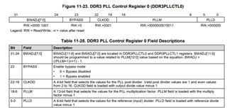
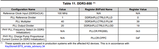
Having gone through the datasheet for the TI Keystone 2 (66AK2E05) part and comparing the DDR3 PLL Control Register 0 bit fields with what is being referenced in DDR3-800 PLL Configuration and DDR3nCLK errata, I have come across two discrepancies/issues. First, the errata refers to a PLL Output Divider (PLLOD) bit field in the DDR PLL control register, but no bit field exists outside of a Clock Output Divider, per the register definition found 66AK2E0x Multicore DSP+ARM KeyStone II System-on-Chip. Assuming the output divider in question is in-fact the Clock Output Divider, the larger issue with the errata is that it states that the register value for the Output Divider should be 19, but the Clock Output Divider field allows for a maximum of 15 (4 bits). Though the math works out, such that the dividers and multiplier do in fact equate to the expected 800 MT/s value, the register does not allow for the specified Output Divider value to be stored in the register field. Is my understanding of the errata flawed, or is this limitation the reason DDR-800 is not recommended for use in production systems?