This thread has been locked.

If you have a related question, please click the "Ask a related question" button in the top right corner. The newly created question will be automatically linked to this question.

PROCESSOR-SDK-AM64X: CPSW3g / CPTS / PHC clock source

Part Number: PROCESSOR-SDK-AM64X

Hi,

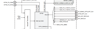
according to https://software-dl.ti.com/processor-sdk-linux-rt/esd/AM64X/07_03_00_02/exports/docs/linux/Foundational_Components/Kernel/Kernel_Drivers/Network/CPSW3g.html#common-platform-time-sync-cpts-module the SDK provides a PTP hardware clock (phc)  in the root fs /dev/ptpN with the following capabilities:

Basic clock operations
   - Set time
   - Get time
   - Shift the clock by a given offset atomically
   - Adjust clock frequency

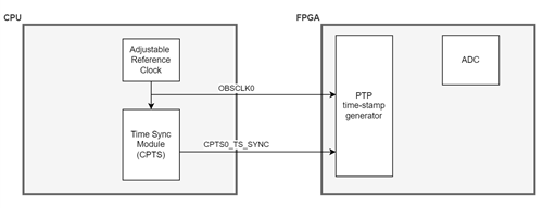
I need to synchronize an external PTP clock (implemented in an FPGA) to that phc clock and I'm wondering if it is possible to output this adjustable clock to the obsclk pin so that it could be used as reference clock in the FPGA
How is the a
djustment of the clock frequency implemented? Fractional PLL or just by skipping or adding clock periods? The CPTS module can be clocked from different clock sources,
which source is used?


Can somebody give me some details how this phc is implemented?

Thank you for your reply!

Best regards
Reto
  • Hello,

    Due to holidays, please expect some delay in response.

    Thanks and regards,

    Jianzhong

  • Schuyler,

    Reto is my customer. Can you please look at that?

    Regards Bernd

  • Hi,

    We are note sure what you are asking. There is a PTP clock derived from ethernet, is this what you want to pass to the FPGA? Or is the clock from the FPGA  that you want to send out? Are you trying to implement a Grand master clock?

    Would you be willing to look at the 8.x AM64 SDK?

    Best Regards,

    Schuyler

  • Hi, thank you for your reply and sorry for my late response! This is what we want to do:

    We have multiple devices that are connected with Ethernet and each of these devices have a CPU running Linux and the ptp4l daemon (The above block diagram is showing one device only). We are doing data acquisition in an FPGA and want to timestamp the acquired data with the PTP time. In order to be able to do that there is an additional PTP clock in the FPGA that generates the time stamps. This FPGA PTP clock must be synchronized with the CPTS module in the AM64x processor.

    My preferred concept was that the CPTS module and the FPGA PTP clock are running from the same (adjustable) clock source. If this was possible it would be sufficient to adjust the phase shift using e.g. the CPTS_TS_SYNC signal.

    So I’m wondering if it is possible to expose the CPTS clock source at the OBSCLK0 pin as drawn in the above block diagram?
    My second question is how the adjustment of the CPTS reference clock is implemented. In order to use it as “PHC” for the ptp4l daemon it must be possible to adjust the clock frequency in very fine steps. Is this done with a fractional PLL or by skipping/adding clock periods?

    Thank you for your reply!

    Best regards

    Reto

  • Hi,

    There is not an adjustable clock source within the device. The CPTS counter can be tuned based on this info here in the AM64x TRM section 10.1.3.4.2 64-bit Timestamp PPM. Please be aware there are several CPTS in the system. One in CPSW, PCIe, System wide CPTS. 

    This TRM section 12.2.1.4.7.11 Timestamp GENFn Output describes an output that can be generated from the CPTS counter and route it to an external pin.  It might be possible to achieve your tuning goal purely with the genf. Please take at this section 12.2.1.4.7.11.1 GENFn Nudge and this section 12.2.1.4.7.11.2 GENFn PPM for tuning ideas. The difference in the two approaches is that the nudge is more of an step tuning and the PPM is the smoothing approach.

    Best Regards,

    Schuyler

  • Hi,
    thank you for your reply! That was very helpful but there still one point that confuses me. I understood that it is possible to generate a tunable clock output using the CPTS_GENFn outputs. The reference for this generated clock is the "CPTS_RFT_CLK" right?

    According to TRM section "12.2.1.4.7.2 CPTS Architecture" the CTPS module inside the CPSW records time stamps for  every packet transmitted or received on external port of the CPSW. Are these time stamps based on the "CPTS_RFT_CLK" too? According the block diagram of the CPTS module I would say yes but to implement  the IEEE 1588-2008 standard I understood that this clock must be tunable. 

    Best regards
    Reto

  • Hi,

    I will need to discuss internally with another team. But for the moment this is what I see for clock adjustment. Are you asking if there is an internal clock that performs like a Vcxo?

    Best Regards,

    Schuyler

  • Hi,
    after reading the CPTS section in the TRM again I realized that the CPSW_CPTS_TS counter is adjusted using the CPSW_CPTS_TS_NUDGE_VAL_REG, CPSW_CPTS_TS_PPM_HIGH_VAL_REG and the CPSW_CPTS_TS_PPM_LOW_VAL_REG registers (In a similar was as the CPSW_GENF outputs). So that question is answered in the meantime, but I have got a new one:

    The processor SDK provides a  Linux kernel driver that allows to generate periodic output signals configurable from user space (Section 3.3.2.5.4.1. Common Platform Time Sync (CPTS) module).

    - These signals are derived from the (adjusted) CPSW_CPTS_TS counter, correct?
    - Which output of the CPTS module is used for these signals? CPTS0_TS_COMP or CPTS0_TS_SYNC or both of them?

    Best regards
    Reto