This thread has been locked.
If you have a related question, please click the "Ask a related question" button in the top right corner. The newly created question will be automatically linked to this question.
Hello
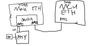
I have 2 RMII in Main-domain shown below, one goes to a 100 base T1 PHY, another one goes to MCU-domain Ethernet, and both of them are RMII connection.
my questions are
1. Since I saw the comments in the datasheet shown below. In our application we use AA25 as our CLKOUT, and AD18(RMII_Clock_output) to receive it, does it mean we have to use the clock source from MAC, rather than using the Crystal on the side of Ethernet Phy?
2.Since we have used 2x RMII in Main domain, how is the clock source topology looks like? may I use AA25 to toggle 50MHz clock and feed to AD18 and C24, and an Ethernet Phy at the same time? the driving strength of the AA25 could handle this situation?
1) We do not recommend using the RMII clock output due to jitter concerns and we are in the process of updating the datasheet.
The clock has to be shared b/w the PHY and the MAC. We would recommend using the crystal (meeting the required jitter specs) on the ethernet PHY and sharing it with the MAC.
With a single clk input in the Main domain but with 2x RMII, it may be a challenge to share the clock. I will discuss this and get back.
Hello Shreyas
Thank you very much for your feedback.
For 1), I get your point, we have reserved a crystal on PHY side, so the 2) question may be more critical, since in 1) we have PHY to provide the clcok to main switch, how to serve the clock of RMII between Main domain & MCU domain.
Chuan,
I haven't had the chance to discuss this yet. but, would it be possible to use the crystal shared to the MCU?
Chuan,
This is an interesting situation which probably never encountered before.
We confirmed looking into the tech reference manual that there is no loopback option of the RMII_REFCLK input back to the CLKOUT.
I discussed this and our suggestion is to use an external clk source that will share the clk with the PHY, MAIN domain (TDA4_1), and the MCU domain(TDA4_2). The drive strength of the external clk source must be taken care and the timing analysis performed such that there is no setup and hold time violations.
There is also an option to have an external clk buffer that can be shared with both TDA4_1 and TDA4_2. Note that timing analysis will still be required to ensure that there is no setup or hold time violations.