Part Number: AM6412
Hi team,
I’ve got question regarding on AM6412 DDR4-SDRAM layout. Could you please take a look below?
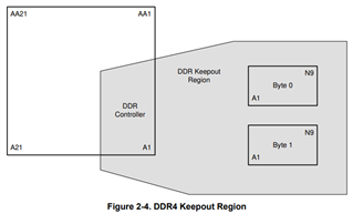
On the Layout Guidelines (here) figure 2-4, SDRAN Byte 0 is shown upper side, and Byte 1 is shown bottom side.

Table 2-5 indicates that BYTE0=DQS0,DQ[7:0] and BYTE1=DQS1,DQ[15:8].

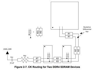
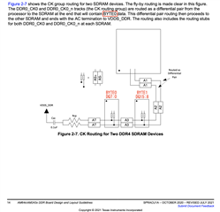
Figure 2-7 also indicates connection from processor to the BYTE0 device.

However, AM6412 has pin configuration which has A1 closed to DQ[7:0] group, and L/M/N closed to DQ[15:8] group. So if I follow the guideline the DQ lines would be crossed.
Right now I’m struggling to understand how the guideline can be followed without crossed lines. Would you please advise? Also, if there is misunderstanding, please let me know.
Best regards,
Kurumi


