


Other Parts Discussed in Thread: OMAP-L138
Hello All,
I'm working on OMAP-L138 custom board now I'm focusing on Processor to FPGA(XC7A200T-2SBG484I) boot. Based on this data sheet (XAPP583) I'm doing booting over FPGA and their provided sample example.
I choose Slave Serial Mode Configuration.
Steps i followed :
1) First i flashed the bit file into memory location with the help of SPI - NOR I just write the bit file in one location and i read it back .
2) Then i downloaded (copy) the bit file into Bit stream start address.
3) I followed the sequence which is mentioned in that datasheet after progressed the bit stream DONE pin is not going High it's always low. I cross verified the configuration timing diagram.
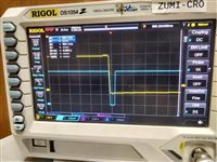
I will attach the Timing diagram and logs which i captured and also i attach the source file. Please refer the figure in the data sheet Figure 5: Serial Configuration Clocking Sequence
Hardware :-
1) We tried 330ohm strong pull up resistor then also DONE pin is always is dead state only
2) Boot pins also we cross verified then also pin is always low.
Please someone help me out of this problem.
PROG_B PROG_B and INIT_B CLOCK and DATA INIT_B and CLOCK


FPGA BOOT LOGS :-
Size target bitstream:
0xc80ffffc: 0x9129a288
First part of target bitstream:
0xc8100000: 0xf00f0900
0xc8100004: 0xf00ff00f
0xc8100008: 0x0000f00f
0xc810000c: 0x30006101
0xc8100010: 0x6e61624c
0xc8100014: 0x58545f64
0xc8100018: 0x64636e2e
0xc810001c: 0x5f57483b
0xc8100020: 0x454d4954
0xc8100024: 0x3d54554f
0xc8100028: 0x534c4146
0xc810002c: 0x73553b45
0xc8100030: 0x44497265
0xc8100034: 0x4678303d
0xc8100038: 0x46464646
0xc810003c: 0x00464646
Last part of target bitstream:
0xc8afffe0: 0x3734e7cb
0xc8afffe4: 0xfbefd6ea
0xc8afffe8: 0x7df8eb55
0xc8afffec: 0xffe29eb8
0xc8affff0: 0x35e9bbfe
0xc8affff4: 0x9f5aaaae
0xc8affff8: 0xff55beae
0xc8affffc: 0xd56daaaa
PROG_B started.
Alpha : Downloading Bitstream to target FPGA
// I cross verified the data in binary
f00f0900
1111 0000 0000 1111 0000 1001 0000 0000
f00ff00f
1111 0000 0000 1111 1111 0000 0000 1111
0000f00f
0000 0000 0000 0000 1111 0000 0000 1111
30006101
0011 0000 0000 0000 0110 0001 0000 0001
6e61624c
0110 1110 0110 0001 0110 0010 0100 1100
58545f64
0101 1000 0101 0100 0101 1111 0110 0100
64636e2e
0110 0100 0110 0011 0110 1110 0010 1110
5f57483b
0101 1111 0101 0111 0100 1000 0011 1011
454d4954
0100 0101 0100 1101 0100 1001 0101 0100
3d54554f
0011 1101 0101 0100 0101 0101 0100 1111
534c4146
0101 0011 0100 1100 0100 0001 0100 0110
73553b45
0111 0011 0101 0101 0011 1011 0100 0101
44497265
0100 0100 0100 1001 0111 0010 0110 0101
4678303d
0100 0110 0111 1000 0011 0000 0011 1101
46464646
0100 0110 0100 0110 0100 0110 0100 0110
0x00464646
0000 0000 0100 0110 0100 0110 0100 0110
/******************************************************************************
 *

 * Xilinx, Inc.
 * XILINX IS PROVIDING THIS DESIGN, CODE, OR INFORMATION "AS IS" AS A
 * COURTESY TO YOU.  BY PROVIDING THIS DESIGN, CODE, OR INFORMATION AS
 * ONE POSSIBLE    IMPLEMENTATION OF THIS FEATURE, APPLICATION OR
 * STANDARD, XILINX IS MAKING NO REPRESENTATION THAT THIS IMPLEMENTATION
 * IS FREE FROM ANY CLAIMS OF INFRINGEMENT, AND YOU ARE RESPONSIBLE
 * FOR OBTAINING ANY RIGHTS YOU MAY REQUIRE FOR YOUR IMPLEMENTATION
 * XILINX EXPRESSLY DISCLAIMS ANY WARRANTY WHATSOEVER WITH RESPECT TO
 * THE ADEQUACY OF THE IMPLEMENTATION, INCLUDING BUT NOT LIMITED TO
 * ANY WARRANTIES OR REPRESENTATIONS THAT THIS IMPLEMENTATION IS FREE
 * FROM CLAIMS OF INFRINGEMENT, IMPLIED WARRANTIES OF MERCHANTABILITY
 * AND FITNESS FOR A PARTICULAR PURPOSE.
 *
 * (c) Copyright 2012 Xilinx, Inc. All rights reserved.
 *
 ******************************************************************************/

/*****************************************************************************
 * Filename:  slave_serial.c
 *
 * Description:
 * Application for processor controlled Slave Serial FPGA configuration
 *
 * MODIFICATION HISTORY:
 *
 * Ver   Who    Date        Changes
 * ----  -----  ----------  ----------------------------------------------------
 * 1.00  mattn  2012-05-21  Initial release
 *
 ******************************************************************************/

/***************************** Include Files *********************************/
#include <stdint.h>
#include <stdio.h>
#include "main.h"

/************************** Constant Definitions *****************************/
/* Account for processor endianness */
//#if __BYTE_ORDER__ == __ORDER_LITTLE_ENDIAN__
#define SWAP_BYTES 0//1
//#else
//#define SWAP_BYTES 0

/* Output GPIO addresses */
//#define CCLK_GPIO_BASEADDR         0x40020000  EMIFA
#define CCLK_GPIO_BASEADDR         0x40020000  //DDR2
#define PROGRAM_B_GPIO_BASEADDR    0x40030000
#define SERIAL_OUT_GPIO_BASEADDR   0x40040000

/* Input GPIO addresses */
#define INIT_B_GPIO_BASEADDR       0x40050000
#define DONE_GPIO_BASEADDR         0x40060000

/* User TODO: Change following #defines to point to the where the bitstream is
 * stored in external memory. This program assumes the first address of
 * external memory contains the size of the target bitstream and the next
 * 32-bit word is the start of the sequentially stored bitstream.
 */
//#define EXT_MEMORY_BASEADDR AXI_SRAM_ADDR
/* Storage location of the size of the bitstream */
#define BITSTREAM_START_ADDR  0xC8100000

/* hardcoded here */
/* Storage location of the size of the bitstream */
/* TBD ! change as required !!!!!!!!!!!!!!!!*/
#define BITSTREAM_SIZE_ADDR 10*1024*1024
//#define BITSTREAM_SIZE_ADDR   0xAEA68C

/******************************************************************************
 * This is the main function Slave Serial configuration example
 *
 * @param    None.
 *
 * @return   0 indicate success, otherwise 1.
 *
 * @note     None.
 *
 ******************************************************************************/

//unsigned char s_tmpwork[128];
int slave_serial(unsigned int bits_start, unsigned int bits_size)
{

    unsigned int i, j;
#if 0
    unsigned int bits_start =  (unsigned int)BITSTREAM_START_ADDR;
    unsigned int bits_size  = *(unsigned int *)BITSTREAM_SIZE_ADDR;

    unsigned int *program_b_ptr = (unsigned int*) PROGRAM_B_GPIO_BASEADDR;  //GPIO6[12] 109
    unsigned int *init_b_ptr = (unsigned int*) INIT_B_GPIO_BASEADDR;        //GPIO6[13] 110
    unsigned int *done_ptr = (unsigned int*) DONE_GPIO_BASEADDR;            //GPIO6[14] 111
    unsigned int *cclk_ptr = (unsigned int*) CCLK_GPIO_BASEADDR;            //GPIO6[15] 112
                                            //serial_out_ptr           DATA //GPIO7[10] 123
#endif

    UARTPuts("\tAlpha : Configuring target FPGA via Slave Serial\r\n", -1);

    //fpga file is actually bits_start!!
   // UARTprintf("Bitstream start address in memory = 0x%08X\n\r", bits_start);
   // UARTprintf("Bitstream size in bytes  = 0x%08X\n\r", bits_size);
#if 1
    UARTprintf("\n\r");
    UARTprintf("Size target bitstream:\n\r");
    UARTprintf("0x%08X: 0x%08X\n\r", bits_start - 4,
               *(uint32_t*) (bits_start - 4));
    UARTprintf("\n\r");
    UARTprintf("First part of target bitstream:\n\r");
    for (i = 0; i < 64; i += 4)
    {
        UARTprintf("0x%08X: 0x%08X\n\r", bits_start + i,
                   *(uint32_t*) (bits_start + i));
    }

    UARTprintf("\n\r");
    UARTprintf("Last part of target bitstream:\n\r");
    j = bits_start + bits_size - 32;

    for (i = j; i < j + 32; i += 4)
    {
        UARTprintf("0x%08X: 0x%08X\n\r", i, *(uint32_t*) i);
    }
    UARTprintf("\n\r");
#endif
    UARTPuts("\tPROG_B started.\r\n", -1);
    /* Configuration Reset */
    GPIOPinWrite(SOC_GPIO_0_REGS, 61, GPIO_PIN_LOW);  //*program_b_ptr = 0
    USTIMER_delay(1);
    //delay(1);
    GPIOPinWrite(SOC_GPIO_0_REGS, 61, GPIO_PIN_HIGH);     //*program_b_ptr = 1
   // UARTPuts("\tPROG_B DONE.\r\n", -1);
#if 1
    /* Wait for Device Initialization */
    i = 0;

    while (GPIOPinRead(SOC_GPIO_0_REGS, 99) == 0) //while(*init_b_ptr == 0)
    {
        /* Timeout and error if INIT_B is slow to goes High */
        ++i;
        if (i > 0x00002000)
        {
            UARTPuts("\tAlpha : INIT_B has not gone high\n\r", -1);
            return 1;
        }
    }
#endif
    /* Configuration (Bitstream) Load */
    UARTPuts("\tAlpha : Downloading Bitstream to target FPGA\n\r", -1);

    for (i = 0; i < bits_size; i += 4)
    {
        shift_word_out(swap_unit32(*(unsigned int*) (bits_start + i)));

    }
#if 1
        if (GPIOPinRead(SOC_GPIO_0_REGS, 99) == 0)  // if (*init_b_ptr == 0)
        {
            UARTPuts("\tAlpha : INIT_B error\n\r", -1);
            return 1;
        }
#endif
    /* Compensate for Special Startup Conditions */
    i = 0;
    int ret;
#if 1
    ret = GPIOPinRead(SOC_GPIO_0_REGS, 63);
    printf("ret = %d\r\n",ret);

    while (GPIOPinRead(SOC_GPIO_0_REGS, 63) == 0) //while(*done_ptr == 0)
    {
        shift_cclk(1);
        /* Timeout and error if DONE fails to go High */
        ++i;
        if (i > 0x00000100)
        {
            UARTPuts("\tAlpha : DONE has not gone high\n\r", -1);
            return 1;
        }
    }
#endif
    shift_cclk(8);

    UARTPuts("\tAlpha : Download Completed\n\r", -1);
    return 0;
}

/******************************************************************************
 * This function serializes a 32-bit word and then clocks each bit on the
 * D01_DIN and CCLK ports of the target
 *
 * @param data32 is the next 32 bits from the bitstream to drive onto the
 * target FPGA's DIN port
 *
 * @return
 *   None
 *
 * @note
 *   The algorithm to shift serially to one a bit wide GPIO is:
 *
 *   for (i = 31; i >= 0; --i){
 *       *serial_out_ptr = (data32 & 1 << i) ? 1 : 0;
 *       shift_cclk(1);
 *   }
 *
 *   However, the below example connects to the D[00:07] port of the target FPGA.
 *   In 7 series FPGA, DIN is the same pin as D[01], therefore, it shifts out
 *   0x40 to this port to assert only the DIN pin:
 *       *serial_out_ptr = (data32 & 1 << i) ? 0x40 : 0;
 *
 ******************************************************************************/
void shift_word_out(unsigned int data32)
{
    //unsigned int * serial_out_ptr = (unsigned int *)SERIAL_OUT_GPIO_BASEADDR;
    int i;

    for (i = 31; i >= 0; --i)
    {
        //*serial_out_ptr = (data32 & 1 << i) ? 0x40 : 0;
        if (data32 & 1 << i)
        {
            GPIOPinWrite(SOC_GPIO_0_REGS, 108, GPIO_PIN_HIGH);
        }
        else
        {
            GPIOPinWrite(SOC_GPIO_0_REGS, 108, GPIO_PIN_LOW);
        }
        shift_cclk(1);
        UARTprintf("%d", (data32 & 1 << i) ? 1 : 0);
    }
    UARTPuts("\n\r", -1);
}

/******************************************************************************
 * swap_unit32() will byte swap an unsigned 32-bit value if the globally
 * defined SWAP_BYTES is 1. This global is set by using GCC predefined macros.
 * See the global defines section for details.
 *
 * @param data is an unsigned 32 bit word
 *
 * @return
 *   If SWAP_BYTES == 1:
 *       unsigned 32 bit byte swapped copy of data parameter
 *   If SWAP_BYTES == 0:
 *       unsigned 32 bit unmodified copy of data parameter
 *
 ******************************************************************************/
unsigned int swap_unit32(unsigned int data)
{
    unsigned int swapped;

    if (SWAP_BYTES == 1)
        swapped = ((data << 24) & 0xFF000000) | ((data << 8) & 0x00FF0000)
                | ((data >> 8) & 0x0000FF00) | ((data >> 24) & 0x000000FF);
    else
        swapped = data;
   // UARTprintf("swapped data = ");
   // UARTprintf("0x%08X: \r\n", swapped );
    return swapped;
}

/******************************************************************************
 * shift_cclk() will assert and then de-assert the CCLK pin
 *
 * @param count is the number of cycles to assert and then de-assert CCLK
 *
 * @return
 *   None
 *
 ******************************************************************************/
void shift_cclk(unsigned int count)
{

    int i;
    // unsigned int * cclk_ptr = (unsigned int *)CCLK_GPIO_BASEADDR;

    for (i = 0; i < count; i++)
    {
        // *cclk_ptr = 1;
        GPIOPinWrite(SOC_GPIO_0_REGS, 107, GPIO_PIN_HIGH);
        // *cclk_ptr = 0;
        GPIOPinWrite(SOC_GPIO_0_REGS, 107, GPIO_PIN_LOW);
    }
}

/******************************************************************************
 * delay() is a simple wait loop. It very roughly matches 1 us on a 75 MHz MB
 * system. Used to make sure PROGRAM_B is asserted long enough

 * @param count is the number of units of time (very roughly 1 us with a 75 MHz
 *   clock) to wait
 *
 * @return
 *   None
 *
 ******************************************************************************/
void delay(int count)
{
    int i;

    int us_adjust = 25;
    for (i = 0; i < count * us_adjust; i++)
        ;
}
Thanks in advance
Regards,
Seyed
