


Part Number: AM4376
Other Parts Discussed in Thread: TMDXSK437X
Hi Team,
I am designing a board using AM4376BZDND30S.
My reference to this Design is: TMDXSK437X (AM437x Starter Kit)
My query is in regard to land pattern for AM4376BZDND30S.
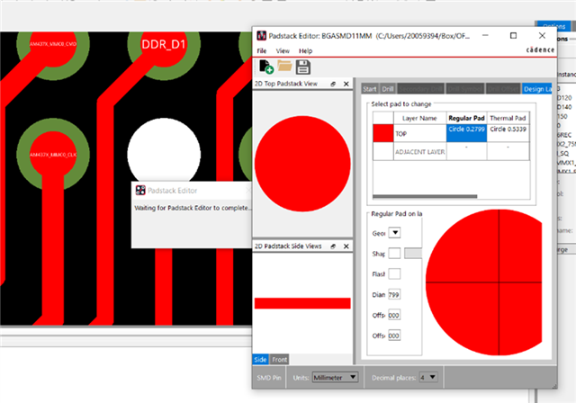
In Starter Kit:
The pad stack for AM437x is 0.2799mm (Land Area to solder)
While referring TI Document - "SPRAA99C – MARCH 2008 – REVISED MAY 2021; Application Report nFBGA Packaging"
Page 7; Table 2-1
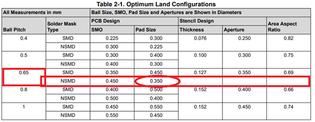
Optimum Land configuration is 0.35mm.
Q1: Pls suggest which land area (pad size) to follow.
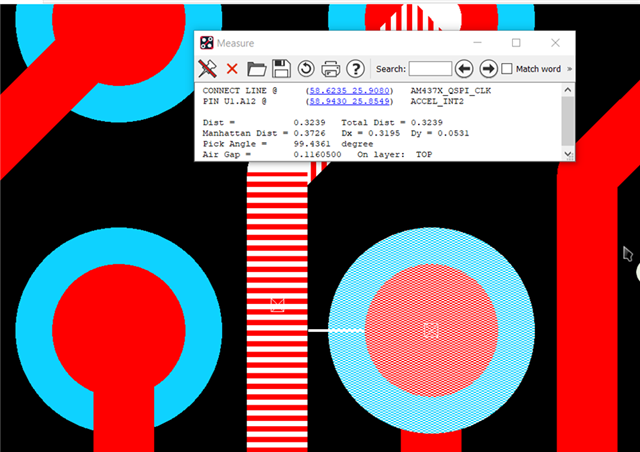
Q2: What should be the minimum air gap that can be between pad and trace. (this will help me decide on the trace width).
Regards,
Siddharth Gupta

