This thread has been locked.

If you have a related question, please click the "Ask a related question" button in the top right corner. The newly created question will be automatically linked to this question.

TDA4VM: Insufficient driving capacity of tda4 rgmii-txd

Part Number: TDA4VM

Hi expert,

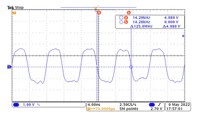
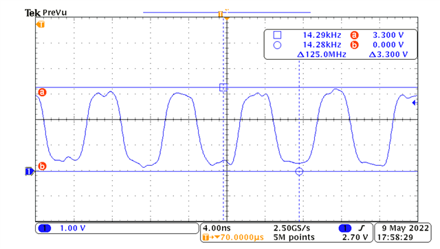
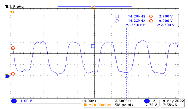
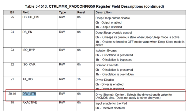
At present, the hardware test indicate that the rgmii TXD data of tda4 shows insufficient driving ability, the level cannot rise to 3.3V, there is no holding time, and the driving ability of the pin is still not improved after modification (the modified register is as follows)
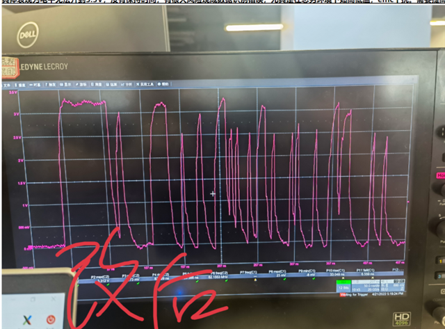
The specific performance is that the level cannot rise to 3.3V, there is no holding time, and there is a great risk of ready-made data identification errors, especially in harsh environments such as high and low temperature and EMC interference. As It is necessary to improve the signal output power of tda4
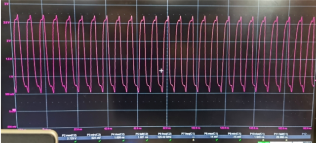
In addition, the output rgmiitx clock signal of tda4 is not good, and there is also the problem of insufficient output capacity, between 0.5-2.7v (normal 0-3.3v)
So is there any way to solve the problem of insufficient rgmii driving ability and whether other information input is needed.
These problems seriously affect the hard test and product stability. Please pay attention and support to solve them. Thank you

  • Dear Jeffrey,

        Please help compare with the clock signal sampled on EVM board.


        It seems your clock is different from what we can see on EVM. Please check the hardware desgin with EVM and software with default SDK.

    Best regards,

    Sikai Lu

  • From looking at the waveform of the original clock measurement - I would guess the probe is not at the receiver, but perhaps at some other point on the trace between source and receiver.  Make sure you are measuring at the load to get the best waveform.  Ensure the probe is properly grounded.  A long ground wire can also affect the measured results.  Lastly - make sure the scope settings are adjusted to properly handle the measured signal (sample rate, resolution, etc.)

  • Hi Robert,

    I work with Jeffrey. We measure the waveform at both receiver (397 side) and source (TDA4 side) many times using a grounding spring (properly grounded), they give same results. The scope settings are already adjusted properly. TDA4 and 397 are directly connected through RGMII interface.

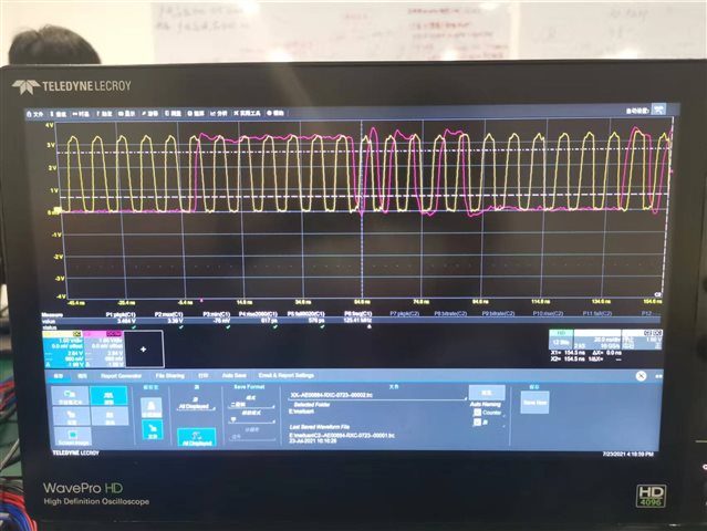
    The following figure is the waveform of 397's output clock (yellow) and data (red) measured at TDA4 side using the same scope and settings. Good signal quality can be found.

    So we are sure that the waveform are properly measured and there is problems in TDA4's ouput signals.

    Best regards,

  • Can you recapture the TDA4 sourced signals at the PHY using the same scope setup and probes? (Same as PHY to TDA4 scope capture).  Be sure to measure directly at the PHY pins.

    Can you provide information abut the RGMII traces (impedance, length, # vias, etc) - or provide the layout for TI to review?

  • Hi Robert,

    First, we are focusing on the internal Ethernet between TDA4 and 397, there is no phy and the connection is MAC to MAC. TDA4 and 397 are directly connected through RGMII interface as follow (TDA4 TX ---- TC397 RX):

    Second, both TDA4 and 397 use BGA packaging, the pins are not accessible. However, some test points close to the pins are reserved and accessible. The measurements are performed exactly at these test points.

    We measured at test points of both sides and got same results. The figures Jeffrey has postted are the waveform at the test point on 397 side.

    The following figure shows distance of RGMII traces:

    All data traces are designed to have the same distance.

    Best regards,

  • The waveform of the clock captured by the customer certainly has some signal integrity artifacts - so its possible the test points are very close to the receiver pins.  In addition - you can see the voltage level difference between that capture an the ones made on our EVM.   The overall length of the RGMII signals do not appear extreme, what impedance are they routed at?  It should be 50-ohms single ended.

  • The impedance are 50-ohms

  • In the original E2E request, you highlighted the DRV_STR bit in the register.  Have you tried adjusting (DS=00 for NOM (approx 60-ohms), DS=01 for FAST, (approx. 50-ohms) DS=10 for SLOW (approx. 90-ohms), DS=11 is reserved.  On our EVM, we use the default setting (DS=00) and do not have issue.

    In you design, do you provide single solid reference/GND plane to provide consistent 50-ohms impedance?  What about the number of vias used?  Note as previously mentioned, you are NOT scoping the signals at the received (but somewhere between transmitter and receiver) - thus you are no seeing the actual signal waveform seen at the receiver.

  • Dear Peng,

         When I was checking this thread for another question, I have found one point that confused me.


         So you want to enforce the ability of W23,25,27,28 ? But if so you should not change the register of padconfig50, you can see from our datasheet the correspond pin of W23 would be PADCONFIG100. 

          I am not sure if I get the right undestanding of your quesiton. Could you help check this for me?

    BR

    Sikai