This thread has been locked.

If you have a related question, please click the "Ask a related question" button in the top right corner. The newly created question will be automatically linked to this question.

66AK2G12: QSPI read access timing

Part Number: 66AK2G12

Hi,

I have a question from my customer for QSPI read timing.
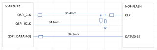
According to datasheet table 5-89, Read setup time is 1.5ns(min).


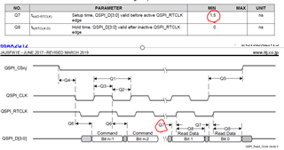
The customer uses QSPI_CLK=96MHz and their Flash memory's "clock low to output valid" parameter is 0 to 6nsec.
So above setup time is not met.

On the other hand, TRM Figure 11-1309 and Table 11-3212 mention QSPI_RD_DATA_CAPTURE_REG[4:1] DELAY_FLD.
It seems the read timing can be adjusted by this parameter using QSPI_REF_CLK which is running *4 QSPI_CLK (which is 384MHz).
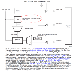


Questions:
Q1) The read timing adjusted by DELAY_FLD bit is not visible at device IO boundary.
So it is OK to ignore the 1.5nsec setup time at IO boundary if data training results is OK?

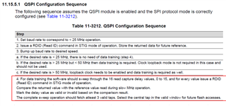
Q2) The configuration sequence says clock loopback should not be used if QSPI_CLK is <50MHz.
What is the reason clock loopback needs to be disabled?

Thanks and regards,
Koichiro Tashiro

  • Hi,

    Any updates for this item? Customer is waiting for an answer.

    Thanks and regards,
    Koichiro Tashiro

  • Hey Koichiro,

    1) As long as the customer is configuring the reference clock to be 4x the output clock, it should be okay. The delay configuration is for the internal sampling of the signal, which uses the reference clock to adjust the sampling point (at 4x the frequency it can be shifted by quarter cycles effectively). That read setup time requirement is specifically for the return/ loopback clock (referred to as RCLK or RTCLK) which may have a different trace length relative to the output clock and bidirectional data pins, so I'd recommend checking with the customer to make sure if they are designing a board that their trace lengths are designed appropriately. Note that the last sentence of 11.15.4.2.1 Read Data Capture makes a point of trace lengths impacting maximum achievable frequency, so the setup time from the memory is less likely to have an impact than the board design itself.

    2) I am not sure of this fully, but my guess is that using the loopback clock must be done with training in order to fine tune the delay in the returned clock; at 25-50MHz the training of internal delays should be enough by itself while at >50MHz output speeds it's used with the training to dial in the results.

    Sincerely,

    Lucas

  • Hi Lucas,

    Thanks for your reply.

    I'd recommend checking with the customer to make sure if they are designing a board that their trace lengths are designed appropriately.

    Below is the trace lengths on customer's board. Do you see any issues here?


    Thanks and regards,
    Koichiro Tashiro

  • Hey Koichiro,

    The only way to know for sure if they're okay is to have the customer run their own signal integrity test simulation using actual PCB characteristics and the IBIS models of each device. 

    Some additional feedback I received from one of our experts is that it's generally not good design practice to connect a device(in this case the flash memory) in the middle of a clock signal PCB trace. This topology can possibly result in the flash device seeing mid-supply voltage steps and create glitches in it's internal clock and logic. 

    Our expert recommended the customer consider an alternative clocking topology; branching the clock signal into two signal traces beginning as close as possible the QSPI_CLK output buffer. Each signal trace would need a series termination resistor located where the signal branches. One signal trace would be routed directly to the QSPI device and the other would be routed to across the PCB to create the desired delay then connected back to QSPI_RCLK. The value of the series termination resistors will need to be adjusted to attenuate reflections returning from the two different signal paths enough that they do not return enough energy down either signal path to cause a problem. 

    Either choice of topology, the best way for the customer to be sure is to have them run their own signal integrity test simulation with their PCB characteristics and use the IBIS models of each device.

    Sincerely,

    Lucas