This thread has been locked.

If you have a related question, please click the "Ask a related question" button in the top right corner. The newly created question will be automatically linked to this question.

TDA4VM: J784S4X - SERDES0 and PCIE REFCLK usage

Part Number: TDA4VM


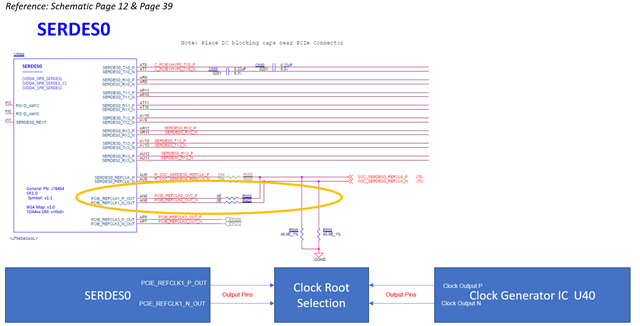
1. Why SERDES0_REFCLK is not used here in the below schematic?

2. PCIE_REFCLK1_OUT is connected to output of Clock generator IC. Both are Output Pins. Please clarify?

Reference Schematic: J784S4X Evaluation Board
Rev: E2
Ver: 3.1
File Name: PROC141E2(001)_SCH
Reference: Schematic Page 12 & Page 39

  • The SERDES_REFCLK can be configured for input or output clock.  However, the clock buffer on the IO is not PCIe compliant.  The PCIe_REFCLK is output clock only and is PCIe compliant.  For PCIe - it is recommended to use the SERDES_REFCLk for PCIe clock input mode and the PCIe_REFCLK output pins for PCIe output clock mode.

  • Question 1. We would like to use SERDES0 lane0 and lane1 for PCIE1 Lane0 & Lane1 interface for SSD.

    Using only PCIe_REFCLK1 output pins for PCIe output clock is sufficient? Don't we need to provide input clock on SERDES0_REFCLK ? Please clarify.

    Refer Below schematic for more details:

    Question 2. 

    We have considered SerDes1, first 2 lanes for PCIE0 (Interface to SoC) and another 2 lanes for SGMII1 & SGMII2.

    Here, you have suggested to ;

     - SGMII1, SGMII2 can use internally generated clock

     - PCIe0 can use externally generated clock input on pins SERDES_REFCLK

     - PCIe_REFCLK_OUT pins will be left unconnected.

    Please confirm on below schematic.

    Question 3:

    In First case (SERDES0), we are using PCIE_REFCLK for clock output and not using SERDES_REFCLK for input. But in second case (SERDES1), we are not using PCIE_REFCLK for clock output and using SERDES_REFCLK for input. Please clarify on this conflicting usage on SERDES. 

  • Question 1: drawing looks correct.  SERDES0 can be used for PCIe1 (2L).  The desire is to have the PCIe_REFCLK to be source from processor and driven to SSD module.  You have selected the correct pins (PCIe_REFCLK1_OUT).  No other connections are needed.  An input clock is not needed on the SERDES_REFCLK pins (clock will be generated internally)

    Question 2:  drawing looks correct.  SERDES1 can be used for both PCIe0 and SGMII1, 2.  Each SERDES can support a maximum of 2 different protocols at a given time (PCIe, SGMII).  Each SERDES can only support a single reference clock from internal clock tree.  Thus if 2nd protocol is used that requires difference freq, then it must be supplied via the SERDES_REFCLK pins.  In this case - internal REFCLK is used for SGMII, external REFCLK is used for PCIe.

    Question 3:  The difference is SERDES0 is supporting a single protocol (PCIe) and SERDES1 is supporting dual protocol (PCIe, SGMII).