


Hi experts
UART0 is used to realize the sending and receiving of serial data,
baud rate: 1.5MHz
start bit: 1
stop bit: 1
data: 8bits,
parity bit: 1.
The configuration code is as follows:
/*
* UART0 EDMA 方式中断接收、发�?
*/
#define am335x
#include "edma_event.h"
#include "uart_irda_cir.h"
#include "soc_AM335x.h"
#include "hw_types.h"
#include "hw_edma3cc.h"
#include "hw_cm_per.h"
#include "hw_control_AM335x.h"
#include "hw_cm_wkup.h"
#include "arch_intc.h"
#include "arch_edma.h"
#include "user_uart0_edma.h"
extern int vm_gui_printf(int x, int y, const char *format, ...);
struct UART_TEST_COUNT
{
unsigned int send_data_count;
unsigned int send_enable_count;
unsigned int send_irq_count;
unsigned int recv_data_count;
unsigned int recv_irq_count;
unsigned int fifo_tx_flag;
}__attribute__((packed));
struct UART_TEST_COUNT G_uart_test_count;
struct UART_FIFO_TX_BUF
{
int tx_interrupt_flag;
int tx_buf_wr;
int tx_buf_rd;
unsigned char *tx_buf;
}__attribute__((packed));
struct UART_FIFO_TX_BUF G_uart_fifo_tx_buf = {0, 0, 0, NULL};
//volatile unsigned int fifo_tx_flag = 0;
unsigned int user_uart0_get_flag(void)
{
return G_uart_fifo_tx_buf.tx_interrupt_flag;
}
/*****************************************************************
UART_fifo_tx_write:
FIFO��ʽ��������ѹ�뻺����
data_p���뻺�������ݵ�ָ��
len���뻺�������ݵij���
******************************************************************/
static void UART_fifo_tx_write(unsigned char *data_p, int len)
{
int i;
if ((data_p == NULL) || (len == 0))
{
return;
}
for (i = 0; i < len; i++)
{
G_uart_fifo_tx_buf.tx_buf[G_uart_fifo_tx_buf.tx_buf_wr] = *data_p;
G_uart_fifo_tx_buf.tx_buf_wr++;
G_uart_fifo_tx_buf.tx_buf_wr &= UART0_TX_BUFF_LOOP;
data_p++;
}
}
/*****************************************************************
UART_fifo_tx_read:
FIFO��ʽ��ȡ������������
data_p����ȡ���������ݵ�ָ��
len����ȡ�����
����ֵ�����������ݳ���
******************************************************************/
static int UART_fifo_tx_read(unsigned char *data_p, int len)
{
int i;
if ((data_p == NULL) || (len == 0))
{
return 0;
}
for (i = 0; i < len; i++)
{
if (G_uart_fifo_tx_buf.tx_buf_rd == G_uart_fifo_tx_buf.tx_buf_wr)
{
break;
}
// ��ȡ����
*data_p = G_uart_fifo_tx_buf.tx_buf[G_uart_fifo_tx_buf.tx_buf_rd];
G_uart_fifo_tx_buf.tx_buf_rd++;
G_uart_fifo_tx_buf.tx_buf_rd &= UART0_TX_BUFF_LOOP;
data_p++;
}
return i;
}
/*****************************************************************
UART_tx_fifo_send_msg:
FIFO��ʽ�������ݷ�����Ϣ�������ⲿ����
data_p�����͵�����ָ��
len�����͵����ݳ���
******************************************************************/
void UART_tx_fifo_send_msg(unsigned char *data_p, int len)
{
unsigned int crt_fifo_data;
int send_len;
if ((data_p == NULL) || (len == 0))
{
return;
}
// ѹ��������
UART_fifo_tx_write(data_p, len);
if (G_uart_fifo_tx_buf.tx_interrupt_flag == 0)
{// û���жϵĻ���ֱ�ӿ��ж�
G_uart_fifo_tx_buf.tx_interrupt_flag = 1;
UARTIntEnable(SOC_UART_0_REGS, UART_INT_THR);
}
}
/*****************************************************************
UART_send_tx_fifo_data:
FIFO��ʽ���ͻ������е����ݣ���η���32������
����ֵ�����η��͵����ݳ���
******************************************************************/
static int UART_send_tx_fifo_data(void)
{
unsigned char send_data[UART0_TX_FIFO_THRE];
int send_len;
send_len = UART_fifo_tx_read(send_data, UART0_TX_FIFO_THRE);
if (send_len > 0)
{
// ��������ж�
UARTFIFOWrite(SOC_UART_0_REGS, send_data, send_len);
G_uart_test_count.send_data_count += send_len;
}
return send_len;
}
void user_uart0_test_count_clr(void)
{
G_uart_test_count.send_data_count = 0;
G_uart_test_count.send_enable_count = 0;
G_uart_test_count.send_irq_count = 0;
G_uart_test_count.recv_data_count = 0;
G_uart_test_count.recv_irq_count = 0;
}
/************************************************************/
//二级缓存;保存等待处理的数据�?
static unsigned char g_uart0_rx_temp[UART0_RX_BUFF_SIZE] = {0};
static unsigned char g_uart0_tx_temp[UART0_TX_BUFF_SIZE] = {0};
static CommRingBuffer g_uart0_rx_ring = {0};
static CommRingBuffer g_uart0_tx_ring = {0};
static unsigned char g_uart0_rx_err = 0; //接收错误,�?�常是接收缓冲满导致数据丢失
//这部分代码来�? AM335X_StarterWare_02_00_01_01 例程
/****************************************************************************/
/* INTERNAL MACROS */
/****************************************************************************/
/* Address of THR and RHR registers of UART. */
#define UART_THR_RHR_REG (SOC_UART_0_REGS)
/* UART Module Input Frequency. */
#define UART_MODULE_INPUT_CLK (48000000)
/* Baud Rate of UART for communication. */
#define BAUD_RATE_115200 (115200)
#define BAUD_RATE_128000 (128000)
#define BAUD_RATE_230400 (230400)
#define BAUD_RATE_460800 (460800)
#define BAUD_RATE_921600 (921600)
/* EDMA3 Event queue number. */
#define EVT_QUEUE_NUM (0)
/* PaRAM Set number for Dummy Transfer. */
#define DUMMY_CH_NUM (5)
/* Wrapper Definitions. */
#define UART_INSTANCE_BASE_ADD (SOC_UART_0_REGS)
#define EDMA3_UART_TX_CHA_NUM (EDMA3_CHA_UART0_TX)
#define EDMA3_UART_RX_CHA_NUM (EDMA3_CHA_UART0_RX)
#define UART_INT_NUM (SYS_INT_UART0INT)
#ifdef UART_ENABLE_FIFO
static void UartFIFOConfigure(void);
#endif
/****************************************************************************/
/* GLOBAL VARIABLES */
/****************************************************************************/
static void (*cb_Fxn[EDMA3_NUM_TCC]) (unsigned int tcc);
/*
** Transmit Trigger Space value. This is applicable only when UART FIFO mode
** is used. Refer to the comments of the API UARTFIFOConfig() to find the
** possible values of TX Trigger Space.
*/
unsigned int txTrigSpace = TX_TRIGGER_SPACE_GRAN_1;
/*
** Number of bytes transmitted by EDMA per TX event sent by UART.
** In UART FIFO mode, this should be equal to the TX Trigger Space value.
*/
unsigned int txBytesPerEvent = TX_BYTES_PER_EVENT;
/*
** Receive DMA Thresold Level. This applies to both UART FIFO and Non-FIFO
** modes of operation. For FIFO mode, refer to the comments of the API
** UARTFIFOConfig() to find the possible values of RX Trigger Level.
** For Non-FIFO mode, this value is 1.
*/
unsigned int rxTrigLevel = RX_DMA_THRESHOLD;
/* Transmit DMA Threshold Level. This is set in TX_DMA_THRESHOLD register. */
unsigned int txThreshLevel = TX_DMA_THRESHOLD;
/*
** This function enables the system L3 and system L4_WKUP clocks.
** This also enables the clocks for UART0 instance.
*/
#if 1
static void UART0ModuleClkConfig(void)
{
/* Configuring L3 Interface Clocks. */
/* Writing to MODULEMODE field of CM_PER_L3_CLKCTRL register. */
HWREG(SOC_CM_PER_REGS + CM_PER_L3_CLKCTRL) |=
CM_PER_L3_CLKCTRL_MODULEMODE_ENABLE;
/* Waiting for MODULEMODE field to reflect the written value. */
while(CM_PER_L3_CLKCTRL_MODULEMODE_ENABLE !=
(HWREG(SOC_CM_PER_REGS + CM_PER_L3_CLKCTRL) &
CM_PER_L3_CLKCTRL_MODULEMODE));
/* Writing to MODULEMODE field of CM_PER_L3_INSTR_CLKCTRL register. */
HWREG(SOC_CM_PER_REGS + CM_PER_L3_INSTR_CLKCTRL) |=
CM_PER_L3_INSTR_CLKCTRL_MODULEMODE_ENABLE;
/* Waiting for MODULEMODE field to reflect the written value. */
while(CM_PER_L3_INSTR_CLKCTRL_MODULEMODE_ENABLE !=
(HWREG(SOC_CM_PER_REGS + CM_PER_L3_INSTR_CLKCTRL) &
CM_PER_L3_INSTR_CLKCTRL_MODULEMODE));
/* Writing to CLKTRCTRL field of CM_PER_L3_CLKSTCTRL register. */
HWREG(SOC_CM_PER_REGS + CM_PER_L3_CLKSTCTRL) |=
CM_PER_L3_CLKSTCTRL_CLKTRCTRL_SW_WKUP;
/* Waiting for CLKTRCTRL field to reflect the written value. */
while(CM_PER_L3_CLKSTCTRL_CLKTRCTRL_SW_WKUP !=
(HWREG(SOC_CM_PER_REGS + CM_PER_L3_CLKSTCTRL) &
CM_PER_L3_CLKSTCTRL_CLKTRCTRL));
/* Writing to CLKTRCTRL field of CM_PER_OCPWP_L3_CLKSTCTRL register. */
HWREG(SOC_CM_PER_REGS + CM_PER_OCPWP_L3_CLKSTCTRL) |=
CM_PER_OCPWP_L3_CLKSTCTRL_CLKTRCTRL_SW_WKUP;
/*Waiting for CLKTRCTRL field to reflect the written value. */
while(CM_PER_OCPWP_L3_CLKSTCTRL_CLKTRCTRL_SW_WKUP !=
(HWREG(SOC_CM_PER_REGS + CM_PER_OCPWP_L3_CLKSTCTRL) &
CM_PER_OCPWP_L3_CLKSTCTRL_CLKTRCTRL));
/* Writing to CLKTRCTRL field of CM_PER_L3S_CLKSTCTRL register. */
HWREG(SOC_CM_PER_REGS + CM_PER_L3S_CLKSTCTRL) |=
CM_PER_L3S_CLKSTCTRL_CLKTRCTRL_SW_WKUP;
/*Waiting for CLKTRCTRL field to reflect the written value. */
while(CM_PER_L3S_CLKSTCTRL_CLKTRCTRL_SW_WKUP !=
(HWREG(SOC_CM_PER_REGS + CM_PER_L3S_CLKSTCTRL) &
CM_PER_L3S_CLKSTCTRL_CLKTRCTRL));
/* Checking fields for necessary values. */
/* Waiting for IDLEST field in CM_PER_L3_CLKCTRL register to be set to 0x0. */
while((CM_PER_L3_CLKCTRL_IDLEST_FUNC << CM_PER_L3_CLKCTRL_IDLEST_SHIFT)!=
(HWREG(SOC_CM_PER_REGS + CM_PER_L3_CLKCTRL) &
CM_PER_L3_CLKCTRL_IDLEST));
/*
** Waiting for IDLEST field in CM_PER_L3_INSTR_CLKCTRL register to attain the
** desired value.
*/
while((CM_PER_L3_INSTR_CLKCTRL_IDLEST_FUNC <<
CM_PER_L3_INSTR_CLKCTRL_IDLEST_SHIFT)!=
(HWREG(SOC_CM_PER_REGS + CM_PER_L3_INSTR_CLKCTRL) &
CM_PER_L3_INSTR_CLKCTRL_IDLEST));
/*
** Waiting for CLKACTIVITY_L3_GCLK field in CM_PER_L3_CLKSTCTRL register to
** attain the desired value.
*/
while(CM_PER_L3_CLKSTCTRL_CLKACTIVITY_L3_GCLK !=
(HWREG(SOC_CM_PER_REGS + CM_PER_L3_CLKSTCTRL) &
CM_PER_L3_CLKSTCTRL_CLKACTIVITY_L3_GCLK));
/*
** Waiting for CLKACTIVITY_OCPWP_L3_GCLK field in CM_PER_OCPWP_L3_CLKSTCTRL
** register to attain the desired value.
*/
while(CM_PER_OCPWP_L3_CLKSTCTRL_CLKACTIVITY_OCPWP_L3_GCLK !=
(HWREG(SOC_CM_PER_REGS + CM_PER_OCPWP_L3_CLKSTCTRL) &
CM_PER_OCPWP_L3_CLKSTCTRL_CLKACTIVITY_OCPWP_L3_GCLK));
/*
** Waiting for CLKACTIVITY_L3S_GCLK field in CM_PER_L3S_CLKSTCTRL register
** to attain the desired value.
*/
while(CM_PER_L3S_CLKSTCTRL_CLKACTIVITY_L3S_GCLK !=
(HWREG(SOC_CM_PER_REGS + CM_PER_L3S_CLKSTCTRL) &
CM_PER_L3S_CLKSTCTRL_CLKACTIVITY_L3S_GCLK));
/* Configuring registers related to Wake-Up region. */
/* Writing to MODULEMODE field of CM_WKUP_CONTROL_CLKCTRL register. */
HWREG(SOC_CM_WKUP_REGS + CM_WKUP_CONTROL_CLKCTRL) |=
CM_WKUP_CONTROL_CLKCTRL_MODULEMODE_ENABLE;
/* Waiting for MODULEMODE field to reflect the written value. */
while(CM_WKUP_CONTROL_CLKCTRL_MODULEMODE_ENABLE !=
(HWREG(SOC_CM_WKUP_REGS + CM_WKUP_CONTROL_CLKCTRL) &
CM_WKUP_CONTROL_CLKCTRL_MODULEMODE));
/* Writing to CLKTRCTRL field of CM_PER_L3S_CLKSTCTRL register. */
HWREG(SOC_CM_WKUP_REGS + CM_WKUP_CLKSTCTRL) |=
CM_WKUP_CLKSTCTRL_CLKTRCTRL_SW_WKUP;
/*Waiting for CLKTRCTRL field to reflect the written value. */
while(CM_WKUP_CLKSTCTRL_CLKTRCTRL_SW_WKUP !=
(HWREG(SOC_CM_WKUP_REGS + CM_WKUP_CLKSTCTRL) &
CM_WKUP_CLKSTCTRL_CLKTRCTRL));
/* Writing to CLKTRCTRL field of CM_L3_AON_CLKSTCTRL register. */
HWREG(SOC_CM_WKUP_REGS + CM_WKUP_CM_L3_AON_CLKSTCTRL) |=
CM_WKUP_CM_L3_AON_CLKSTCTRL_CLKTRCTRL_SW_WKUP;
/*Waiting for CLKTRCTRL field to reflect the written value. */
while(CM_WKUP_CM_L3_AON_CLKSTCTRL_CLKTRCTRL_SW_WKUP !=
(HWREG(SOC_CM_WKUP_REGS + CM_WKUP_CM_L3_AON_CLKSTCTRL) &
CM_WKUP_CM_L3_AON_CLKSTCTRL_CLKTRCTRL));
/* Writing to MODULEMODE field of CM_WKUP_UART0_CLKCTRL register. */
HWREG(SOC_CM_WKUP_REGS + CM_WKUP_UART0_CLKCTRL) |=
CM_WKUP_UART0_CLKCTRL_MODULEMODE_ENABLE;
/* Waiting for MODULEMODE field to reflect the written value. */
while(CM_WKUP_UART0_CLKCTRL_MODULEMODE_ENABLE !=
(HWREG(SOC_CM_WKUP_REGS + CM_WKUP_UART0_CLKCTRL) &
CM_WKUP_UART0_CLKCTRL_MODULEMODE));
/* Verifying if the other bits are set to required settings. */
/*
** Waiting for IDLEST field in CM_WKUP_CONTROL_CLKCTRL register to attain
** desired value.
*/
while((CM_WKUP_CONTROL_CLKCTRL_IDLEST_FUNC <<
CM_WKUP_CONTROL_CLKCTRL_IDLEST_SHIFT) !=
(HWREG(SOC_CM_WKUP_REGS + CM_WKUP_CONTROL_CLKCTRL) &
CM_WKUP_CONTROL_CLKCTRL_IDLEST));
/*
** Waiting for CLKACTIVITY_L3_AON_GCLK field in CM_L3_AON_CLKSTCTRL
** register to attain desired value.
*/
while(CM_WKUP_CM_L3_AON_CLKSTCTRL_CLKACTIVITY_L3_AON_GCLK !=
(HWREG(SOC_CM_WKUP_REGS + CM_WKUP_CM_L3_AON_CLKSTCTRL) &
CM_WKUP_CM_L3_AON_CLKSTCTRL_CLKACTIVITY_L3_AON_GCLK));
/*
** Waiting for IDLEST field in CM_WKUP_L4WKUP_CLKCTRL register to attain
** desired value.
*/
while((CM_WKUP_L4WKUP_CLKCTRL_IDLEST_FUNC <<
CM_WKUP_L4WKUP_CLKCTRL_IDLEST_SHIFT) !=
(HWREG(SOC_CM_WKUP_REGS + CM_WKUP_L4WKUP_CLKCTRL) &
CM_WKUP_L4WKUP_CLKCTRL_IDLEST));
/*
** Waiting for CLKACTIVITY_L4_WKUP_GCLK field in CM_WKUP_CLKSTCTRL register
** to attain desired value.
*/
while(CM_WKUP_CLKSTCTRL_CLKACTIVITY_L4_WKUP_GCLK !=
(HWREG(SOC_CM_WKUP_REGS + CM_WKUP_CLKSTCTRL) &
CM_WKUP_CLKSTCTRL_CLKACTIVITY_L4_WKUP_GCLK));
/*
** Waiting for CLKACTIVITY_L4_WKUP_AON_GCLK field in CM_L4_WKUP_AON_CLKSTCTRL
** register to attain desired value.
*/
while(CM_WKUP_CM_L4_WKUP_AON_CLKSTCTRL_CLKACTIVITY_L4_WKUP_AON_GCLK !=
(HWREG(SOC_CM_WKUP_REGS + CM_WKUP_CM_L4_WKUP_AON_CLKSTCTRL) &
CM_WKUP_CM_L4_WKUP_AON_CLKSTCTRL_CLKACTIVITY_L4_WKUP_AON_GCLK));
/*
** Waiting for CLKACTIVITY_UART0_GFCLK field in CM_WKUP_CLKSTCTRL
** register to attain desired value.
*/
while(CM_WKUP_CLKSTCTRL_CLKACTIVITY_UART0_GFCLK !=
(HWREG(SOC_CM_WKUP_REGS + CM_WKUP_CLKSTCTRL) &
CM_WKUP_CLKSTCTRL_CLKACTIVITY_UART0_GFCLK));
/*
** Waiting for IDLEST field in CM_WKUP_UART0_CLKCTRL register to attain
** desired value.
*/
while((CM_WKUP_UART0_CLKCTRL_IDLEST_FUNC <<
CM_WKUP_UART0_CLKCTRL_IDLEST_SHIFT) !=
(HWREG(SOC_CM_WKUP_REGS + CM_WKUP_UART0_CLKCTRL) &
CM_WKUP_UART0_CLKCTRL_IDLEST));
}
#endif
unsigned char rxByte;
static void UARTIsr(void)
{
unsigned int intId = 0;
unsigned int i;
unsigned int rx_len;
/* Checking ths source of UART interrupt. */
intId = UARTIntIdentityGet(UART_INSTANCE_BASE_ADD);
UARTIntDisable(SOC_UART_0_REGS, UART_INT_THR);
switch(intId)
{
case UART_INTID_TX_THRES_REACH: // ��������ж�
G_uart_test_count.send_irq_count++;
UART_send_tx_fifo_data();
if (G_uart_fifo_tx_buf.tx_buf_rd == G_uart_fifo_tx_buf.tx_buf_wr)
{// û�������ˣ��رշ����ж�
G_uart_fifo_tx_buf.tx_interrupt_flag = 0;
}
break;
case UART_INTID_RX_THRES_REACH:
G_uart_test_count.recv_irq_count++;
// rx_len = UARTRxFIFOLevelGet(UART_INSTANCE_BASE_ADD);
// if (rx_len > 8)
// {
// rx_len = 8;
// }
G_uart_test_count.recv_data_count += 8;
for (i = 0; i < 8; i++)
{
rxByte = UARTFIFOCharGet(UART_INSTANCE_BASE_ADD);
}
break;
default:
break;
}
if (G_uart_fifo_tx_buf.tx_interrupt_flag)
{
UARTIntEnable(SOC_UART_0_REGS, UART_INT_THR);
}
}
static void UARTINTCConfigure(void)
{
/* Initializing the ARM Interrupt Controller. */
//IntAINTCInit(); //����int arch_core_init(void)��?
/* Registering the Interrupt Service Routine(ISR). */
//IntRegister(UART_INSTANCE_INT_NUM, UARTIsr);
arch_int_register(SYS_INT_UART0INT, UARTIsr);
/* Setting the priority for the system interrupt in AINTC. */
//IntPrioritySet(UART_INSTANCE_INT_NUM, 0, AINTC_HOSTINT_ROUTE_IRQ);
arch_int_priority(SYS_INT_UART0INT, 0, AINTC_HOSTINT_ROUTE_IRQ);
/* Enabling the system interrupt in AINTC. */
//IntSystemEnable(UART_INSTANCE_INT_NUM);
arch_int_enable(SYS_INT_UART0INT);
}
/*
** This function initializes the UART instance for use.
*/
static void UARTInitialize(void)
{
/* Performing a module reset. */
UARTModuleReset(UART_INSTANCE_BASE_ADD);
/* Performing FIFO settings. */
UartFIFOConfigure();
/* Performing Baud Rate settings. */
UartBaudRateSet();
/* Switching to Configuration Mode B. */
UARTRegConfigModeEnable(UART_INSTANCE_BASE_ADD, UART_REG_CONFIG_MODE_B);
/* Programming the Line Characteristics. */
UARTLineCharacConfig(UART_INSTANCE_BASE_ADD,
(UART_FRAME_WORD_LENGTH_8 | UART_FRAME_NUM_STB_1),
UART_ODD_PARITY);
/* Disabling write access to Divisor Latches. */
UARTDivisorLatchDisable(UART_INSTANCE_BASE_ADD);
/* Disabling Break Control. */
UARTBreakCtl(UART_INSTANCE_BASE_ADD, UART_BREAK_COND_DISABLE);
/* Switching to UART16x operating mode. */
UARTOperatingModeSelect(UART_INSTANCE_BASE_ADD, UART16x_OPER_MODE);
// �����ж�
UARTINTCConfigure();
}
/*
** A wrapper function performing FIFO configurations.
*/
static void UartFIFOConfigure(void)
{
unsigned int fifoConfig = 0;
/*
** Transmitter Trigger Level Granularity is 1.
** Receiver Trigger Level Granularity is 1.
** Transmit Trigger Space set using 'txTrigSpace'.
** Receive Trigger level set using 'rxTrigLevel'.
** Clear the Trasnmit FIFO.
** Clear the Receive FIFO.
** DMA Mode enabling shall happen through SCR register.
** DMA Mode 1 is enabled.
*/
#if 0
fifoConfig = UART_FIFO_CONFIG(UART_TRIG_LVL_GRANULARITY_1,
UART_TRIG_LVL_GRANULARITY_1,
txTrigSpace,
rxTrigLevel,
1,
1,
UART_DMA_EN_PATH_SCR,
UART_DMA_MODE_1_ENABLE);
#endif
fifoConfig = UART_FIFO_CONFIG(UART_TRIG_LVL_GRANULARITY_1,
UART_TRIG_LVL_GRANULARITY_1,
32,
8,
1,
1,
UART_DMA_EN_PATH_SCR,
UART_DMA_MODE_0_ENABLE);
/* Configuring the FIFO settings. */
UARTFIFOConfig(UART_INSTANCE_BASE_ADD, fifoConfig);
}
/*
** A wrapper function performing Baud Rate settings.
*/
static void UartBaudRateSet(void)
{
unsigned int divisorValue = 0;
/* Computing the Divisor Value. */
/*
if(baudRate > 230400 && baudRate < 1500000)
bit13_mode = 1;
user_uart0_edma_init
*/
divisorValue = UARTDivisorValCompute(UART_MODULE_INPUT_CLK,
BAUD_RATE_USER,
UART16x_OPER_MODE,
UART_MIR_OVERSAMPLING_RATE_42);
/* Programming the Divisor Latches. */
UARTDivisorLatchWrite(UART_INSTANCE_BASE_ADD, divisorValue);
}
//64字节对齐
//#ifdef __IAR_SYSTEMS_ICC__
#pragma data_alignment=64
static volatile unsigned char g_uart0_tx_buff[64] = {0};
//#endif
//64字节对齐
//#ifdef __IAR_SYSTEMS_ICC__
#pragma data_alignment=64
static volatile unsigned char g_uart0_rx_buff[UART0_RX_CH_COUNT][64] = {0};
//#endif
//每个通道号对应的 buff地址
static unsigned char * g_uart0_rx_ptr[EDMA3_NUM_TCC] = {0};
// �����ʼ�����
void user_uart0_edma_init()
{
uart0_rx_init();
uart0_tx_init();
/* Configuring the system clocks for EDMA. */
//EDMAModuleClkConfig(); //已在arch_edma_init()中调�?
/* Configuring the system clocks for UART0 instance. */
UART0ModuleClkConfig();
/* Performing Pin Multiplexing for UART0 instance. */
//UARTPinMuxSetup(0);
/* Enabling IRQ in CPSR of ARM processor. */
//IntMasterIRQEnable(); //已在int arch_core_init(void)中调�?
/* Initializing the ARM Interrupt Controller. */
//IntAINTCInit(); //已在int arch_core_init(void)中调�?
/* Initializing the EDMA. */
//EDMA3Initialize();
//EDMA3INTCConfigure();
/* Initializing the UART0 instance for use. */
UARTInitialize();
/*
** Configuring the EDMA.
*/
#if 0
/* Request DMA Channel and TCC for UART Transmit*/
EDMA3RequestChannel(SOC_EDMA30CC_0_REGS, EDMA3_CHANNEL_TYPE_DMA,
EDMA3_UART_TX_CHA_NUM, EDMA3_UART_TX_CHA_NUM,
EVT_QUEUE_NUM);
/* Registering Callback Function for TX*/
cb_Fxn[EDMA3_UART_TX_CHA_NUM] = &callback_uart0_edma_send_isr;
//��ʼ�����������??
uart0_edma_rx_channel_init();
#endif
// �����ж�
UARTIntEnable(UART_INSTANCE_BASE_ADD, UART_INT_RHR_CTI);
}
During the UART0 self-loop test (the transceiver line is directly short-circuited), if the data sent continuously is greater than 64 bytes, a crash will occur. In the test, every time 72 bytes are sent, there must be a crash.
Debugging process:
1. Sender:
Do not use DMA, set the send interrupt trigger threshold to 32, and automatically transfer data to the FIFO after triggering the interrupt, each time no more than 32 bytes; until the buffer has no data; the buffer size is currently defined as 32768.
Debugging: no self-looping, there is no problem in sending 960 bytes continuously every 10 milliseconds, and there will be no crash phenomenon; the oscilloscope observes the data, and there is no problem. Basically eliminate the problem of the sender.
2. Receiver:
Do not use DMA, set the receive interrupt trigger threshold to 8, and directly read the data in the 8 FIFOs after each interrupt is triggered. At present, it seems that the receiving end causes
Debugging: As an interrupt problem was suspected, an output pin on the board was set as a test to indicate the process of receiving interrupt processing. Enter the receive interrupt, the pin is pulled low; the interrupt processing is completed, the pin is pulled high.
(1) Continuously receive data equal to 64 bytes:
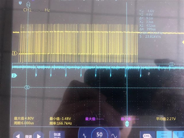
It can be seen that the processing of the 8 receiving interrupts is basically in line with the design expectations. At this time, the ARM will not crash.
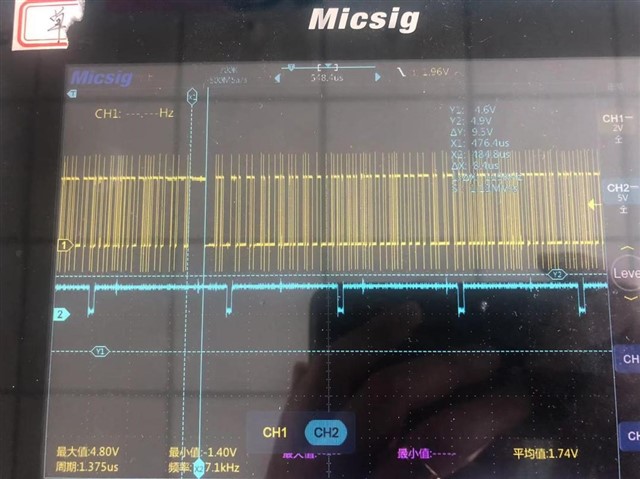
(2) Continuously receive data equal to 72 bytes:
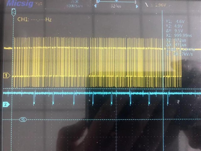
You can see 8 interrupts on the oscilloscope; after the eighth interrupt, there is still data, and there should be 8 bytes to trigger another interrupt, but it has crashed at this time, and the ninth interrupt has not come.
(3) Continuously receive data equal to 128 bytes:
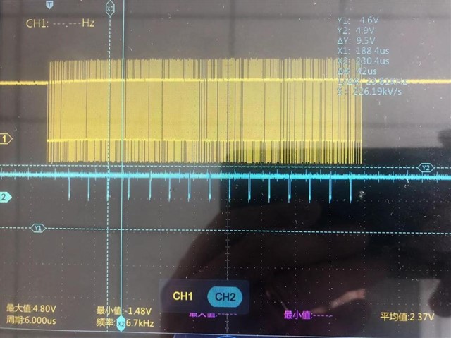
15 interrupts can be seen on the oscilloscope; after the 15th interrupt, there is still data, and there should be 8 bytes to trigger another interrupt, but it has crashed at this time, and the 16th interrupt has not come.
(4) The compartment receives 2 consecutive 64-byte data:
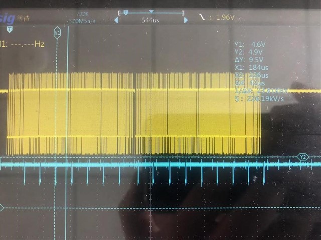
Send two 64-byte data in a row, with a deliberate interval in between.
16 interrupts can be seen on the oscilloscope; reception is normal, no crashes.
The interval between two consecutive data is about 8us:
From what I have seen so far, it seems that the receiving end of UART0 cannot receive continuous data larger than 64 bytes; please help me to see if it is a setting problem?
BR
Ethan
