This thread has been locked.

If you have a related question, please click the "Ask a related question" button in the top right corner. The newly created question will be automatically linked to this question.

66AK2G12: Parallel NOR flash XIP reboot

Part Number: 66AK2G12
Other Parts Discussed in Thread: SYSCONFIG

Hello,

I am trying to fix warm reset issue of our custom board. We need to have a possibility to restart the target system from a SW application and re-run our preloader located in the parallel NOR flash memory (NOR).
The preloader successfully runs after Power On Reset (POR), the GPMC is properly configured, contents of the NOR flash can be seen at the expected memory area (0x3003E000).

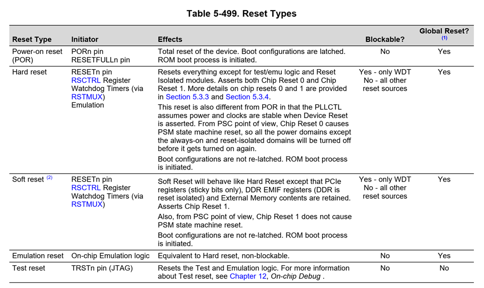
The first method was trigger the warm reset (RST) by setting zero value to the 'SWRST' bit of the 'RSCTRL' register, either Hard reset as call sequence:

volatile DWORD* rsctrl = (DWORD*)RSCTRL;
*rsctrl = RSCTRL_KEY;
*rsctrl = RSCTRL_RESET;

or Soft reset:

volatile DWORD* rsctrl = (DWORD*)RSCTRL;
*rsctrl = RSCTRL_KEY;
((DWORD)RSCFG) |= 0x00003000UL;
*rsctrl = RSCTRL_KEY;
*rsctrl = RSCTRL_RESET;

where:

#define RSCTRL_OFFSET 0x000000E8UL
#define RSCTRL (PLLC_CFG_REGS + RSCTRL_OFFSET)
#define RSCTRL_KEY 0x00005A69UL
#define RSCTRL_RESET 0UL
#define RSCFG (PLLC_CFG_REGS + 0x000000ECUL)

For both Soft and Hard resets the result is the same. After the RST, the same memory area is filled by zeroes and 'GPMC_ERR_' registers are nonzero:

GPMC_ERR_ADDRESS = 0x34000000
GPMC_ERR_TYPE        =  0x00000211

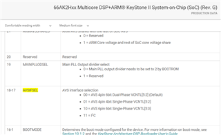
The 'BOOTCFG_' registers contain expected values, especially the 'BOOTCFG_DEVSTAT' corresponds to the strap pins, setting the boot mode and its parameters:

BOOTCFG_DEVSTAT = 0x00060395

It seems the processor is reset (the emulator probe was disconnected), I also verified the RESET pin of the NOR device is pulsed. When in such unstable state of the NOR access, I connected to the SoC the emulator back and invoked Board Setup (PLL setup, etc.) function in GEL from CCS, the Memory Browser momentarily shown valid data at the given address space, but then all was filled with the '0xFFFFFFFF' pattern.

According to errata 66AK2G12 'KeyStoneII.BTS_errata_advisory.46 BOOT, GPMC: GPMC XIP Boot Failure' the strap pins select 100 MHz PLL reference clock, so the GPMC uses less aggressive timing when accessing the NOR device during boot process, then it is up to the higher boot stages to reconfigure to the right timing when BootROM succeeded reading Preloader. I added a code setting the timing back similarly as selected by strap pins before the RST is triggered, but it causes also NOR access loss. I tried to modify 'BOOTCFG_DEVSTAT' register to set 25 MHz PLL reference for normal timing instead of the errata workaround, but the strap pins are latched back into the 'BOOTCFG_DEVSTAT' after RST, even though it is written in the 66AK2G12 TRM that it should occur after the POR only.

The second method was modify the Boot Parameter Table to play with the GPMC configuration, then jump onto the BootROM re-entry function at address 0x00001004, to mimic the two-stage boot, but the CPU is trapped in the infinite loop at address 0x00000B88: 'E12FFF1E   bx  lr'.
I tried to set zero value at the ARMSS BOOT_MAGIC_ADDRESS, before the jump to re-entry, but the result is the same:

static volatile xipBootParams_t* bootParams = reinterpret_cast<xipBootParams_t*>(0x0C0F4100);
bootParams->options = 1;
bootParams->gpmcConfig1_msw = 0x0000;
bootParams->gpmcConfig1_lsw = 0x1002;
bootParams->gpmcConfig2_msw = 0x0010;
bootParams->gpmcConfig2_lsw = 0x1001;
bootParams->gpmcConfig3_msw = 0x2206;
bootParams->gpmcConfig3_lsw = 0x0514;
bootParams->gpmcConfig4_msw = 0x1005;
bootParams->gpmcConfig4_lsw = 0x7016;
bootParams->gpmcConfig5_msw = 0x010F;
bootParams->gpmcConfig5_lsw = 0x1111;
bootParams->gpmcConfig6_msw = 0x8F07;
bootParams->gpmcConfig6_lsw = 0x0000;
bootParams->gpmcConfig7_msw = 0x0000;
bootParams->gpmcConfig7_lsw = 0x0C70;
bootParams->gpmcConfig_msw = 0x0000;
bootParams->gpmcConfig_lsw = 0x0A00;


//*((DWORD*)0x0C0F0000) = 0UL; // ARMSS BOOT_MAGIC_ADDRESS
((void(*)(void))0x00001004)();

Unfortunatelly, I do not see under the hood of SoC's BootROM what is happenning there, so I cannot troubleshoot it. I am not sure what all is required before jump to the BootROM re-entry, to avoid any such infinite loop trap, also what is the purpose of the 'ARMSS BOOT_MAGIC_ADDRESS'. I tried to call '_romtDeviceFreqMHz()' at address 0x00001020 and got expected value without any crash, just to be sure I call BootROM functions properly.

How can I reset from our application without cold/hardware reset?

Thank you for your support,

Jiri

  • Jiri, i will need some time to investigate.  I know this is not an final option for you, but have you tried the warm reset pin RESETn?  Just wondering if that works, it will help narrow down the issue.

    Regards,

    James

  • Hello James,

    I momentarily pulled the RESETn (W3) pin down, and the effect is the same as triggering by the 'RSCTRL' register, the RESETSTATn (Y2) pin pulses, so the NOR device is reset by that signal, after the emulator reconnection I can see zeroes at the address where the NOR is mapped. I can return back to the proper state after POR only.

    Thanks,

    Jiri

  • ok thanks.  Still looking into it...

  • I think possibly the PLL that drives GPMC is getting reset isolated.  So when the boot ROM executes, the frequency is not as expected and the boot fails.  Especially considering the errata you cited, this PLL needs to be set correctly using the info from the BOOTCFG pins.  Can you ensure the PLL associated with GPMC is not reset isolated in the RSISO register? 

    You are correct that the warm reset should not be re-latching the boot pins, so the original BOOTCFG_DEVSTAT should remain.

    Regards,

    James


  • Hello,

    I read the RSISO register, there is 0x00000001 value before I triggered the warm reset, I expect the least significant bit is not related to the GPMC. I have also set the RSISO to zero, so no reset is isolated, the result is a bit worse, when I try to perform the Board Setup function in GEL, I will get 'Could not read register CP15_Registers.REG_CTXA15_CP15_C0_MPIDR: execution state prevented access at (REG_CTXA15_CP15_C0_MPIDR&0x3)' error. The POR is the only way how to get it running properly again. I also cleared the bit 'RESETISO' in MDCTL9 register, the situation is the same as if I do not change anything related to the reset isolation.

    I have found, according to section '5.3.3 Hard Reset' in TRM, the hard reset shall reset neither test nor emulation logic. An emulator session should continue unaffected. But, after the warm reset, I get 'CortexA15: Error: (Error -1170 @ 0x0) Unable to access the DAP. Reset the device, and retry the operation. If error persists, confirm configuration, power-cycle the board, and/or try more reliable JTAG settings (e.g. lower TCLK). (Emulation package 9.6.0.00172) ' error message, the emulator is disconnected, then I need to re-connect the emulator manually for debugging.

    I changed value in the DEVSTAT register before the RST is triggered, unfortunately, that custom value is overwritten (re-latched) back to the corresponding one from BOOTCFG pins after the reset.

    Regards,

    Jiri

  • Jiri

    James is out of the office until early next week.   While he is out,  I will see if I can find additional information for you..

    --Paul 

  • Hi PaulM, did you manage to find any additional information?

  • Hi Andy, I'm not sure why you are seeing this behavior

    One suspicious thing may be the reset signal to the NOR.  Maybe the timing for that signal isn't correct or putting the NOR in a bad state.  Is it possible to modify the board to remove the reset pulse to the NOR during warm reset?  

    Can you compare the GPMC configuration after a POR and a warm reset?  At this point, I would not worry about trying to boot after a warm reset, just see if you can get proper access after a warm reset, by performing tests via JTAG.  From what you are describing, it seems the NOR is in a weird state, or something is fundamentally wrong with the GPMC controller configuration.

    Are you able to probe some signals on the interface?  Just to get an idea that the timing is similar after a POR and after a warm reset?

    Regards,

    James


  • Hi James,

    Thanks for getting back to me.  We have code running on a CPU that we wish to trigger the reset from.  When connected to the target via the DSP, I am able to read the GPMC registers in the register window and memory browser.  After a reset, I resume the target connection and can see the values in both the register view and memory browser with auto-refresh on.  The values have not changed.  On occasion, it has stated that the target is held in reset.  I am unable to view the values when connected to the CPU.

    What specifically would you like me to try and probe on the interface?

  • Hi Andy, let me clarify your statements.  Is this correct:

    CCS connected to C66x: Can view GPMC registers before and after warm reset

    CCS connected to A15: Can only view GPMC register before warm reset.  Is there an error connecting to the A15 after the warm reset, or just a problem viewing the GPMC regs.

    As for probing the interface, i guess let's just start with simply checking to see if CS goes active or you can detect read activity on the read strobe after a warm reset.

    Regards,

    James

  • Hi James,

    I power on the card, connect to the target via the C66x and resume it.  I can see the GPMC registers.  I perform a warm reset, the connection stalls so I resume it again and can still see the GPMC register values in both windows

    If I power on the card having connected the target to the A15 and resume the connection, I cannot read the GPMC registers at all.  With auto-refresh on, it looks like it attempts to read the GPMC_CONFIG register periodically but I get "Error: unable to read" in the register window.  After performing a warm reset, the connection doesn't stall like on the C66x, it remains running and the following errors are present in the console:

    CortexA15: Error: (Error -1170 @ 0x0) Unable to access the DAP. Reset the device, and retry the operation. If error persists, confirm configuration, power-cycle the board, and/or try more reliable JTAG settings (e.g. lower TCLK). (Emulation package 9.6.0.00172)
    CortexA15: Trouble Halting Target CPU: (Error -2064 @ 0x0) Unable to read device status. Reset the device, and retry the operation. If error persists, confirm configuration, power-cycle the board, and/or try more reliable JTAG settings (e.g. lower TCLK). (Emulation package 9.6.0.00172)
    CortexA15: Unable to determine target status after 20 attempts
    CortexA15: Failed to remove the debug state from the target before disconnecting. There may still be breakpoint op-codes embedded in program memory. It is recommended that you reset the emulator before you connect and reload your program before you continue debugging

    The register window still displays the same "Error: unable to read".

    I'll look at probing the interface.

    Many thanks,

    Andy

  • Hi Andy, something seems to be fundamentally wrong in your JTAG connection.  You should be able to see the GPMC registers from the A15.  In the first part of this thread:

    The preloader successfully runs after Power On Reset (POR), the GPMC is properly configured, contents of the NOR flash can be seen at the expected memory area (0x3003E000).

    but now that doesn't seem to be the case.  Has something changed?  Would like to get this understood before debugging the warm reset issue, it may be clue.

    Regards,

    james

  • Hi James,

    I have changed the jtag from a spectrum to a blackhawk checked and then swapped the card for a different one and get the same behaviour, "Error: Unable to read" in the Registers window, "????????" in the memory browser.  I am checking register 0x21818000 area as per the 66AK2G1x technical reference manual.  However, I am also unable to read 0x3003E000, I just get "???????" in the memory browser.

    All of this is when the connection to the target is resumed.  It seems that once suspended I can see the memory values. So can only see memory values when the connection to the target is suspended.  I could see register values with the connection to the target resumed when connected to the C66.

    Jiri will have a different physical set of components to me as we aren't in the same country.

  • Andy, are you doing any cross triggering in your debugger?

    When the A15 is executing code, it won't be able to read register or memory contents.  The core has to be sitting at a breakpoint or code execution has to be stopped in order to read registers/memory.  Is that what is going on?

    Back to the warm reset, does the CS signal to the memory toggle after a warm reset?  This will indicate that the device is attempting to boot from the NOR

    Also, what is the behavior of the NOR reset signal.  What is it's relationship with the RESETSTATn signal when the warm reset is triggered?

    REgards,

    James

  • Hi James,

    The code is just running natively when I try to evaluate the register values, the connection to the target is established purely to check those register values.  It sounds like that issue is more user error than anything else then.  But in short, in that case, yes I can read the registers but have the connection issue when performing the warm reset as it drops.

    I will see what options we have for checking the signals and get back to you.

    Many thanks,

    Andy

  • OK, that probably makes sense.  CCS can be cumbersome across resets, so this is probably expected behavior.  

    Checking the signals will just confirm that it is attempting to boot from the NOR flash, as it does successfully from POR.  Comparing key signals like CS or read strobe between a successful boot and after a warm reset will tell us how far into the boot it progresses after warm reset.

    Regards,

    James

  • Hi James,

    I have probed the chip select for the nor flash.  I can see a change in voltage with a POR maxing at around 700mv.  When I perform the warm reset via code, no noticeable change is seen at all.

    Is approx. 700mv peak too low? looking at the data sheets, I see values of 3.3V for CSn0 mentioned.

    Many thanks,

    Andy

  • Andy, yes 700mV isn't correct, that voltage swing should be to whatever the IO voltage is set to (probably 3.3V for your board).  Can you check the IO voltage and if there are other voltage conflicts on that signal?

    Regards,

    James

  • Hi James,

    Not sure what was happening before, but have checked the CSn0 again with a probe.  I can see the voltage change of approx 3.3V.  We have the boot pins configured for XIP and with POR see an initial voltage of 0V, raising to 3.3V once we are booted successfully.  When I perform a warm reset via code, I don't see a voltage change at all.  It remains at 3.3V as it did once booted from cold.

    Many thanks,

    Andy

  • Hi James,

    Further to this, I have captured the GPMC registers before and after the warm reset via the C66 using a gel script:

    BEFORE:

    C66xx: GEL Output: REVISION: 0x21818000 0x00000060
    C66xx: GEL Output: SYSCONFIG: 0x21818010 0x00000000
    C66xx: GEL Output: SYSSTATUS: 0x21818014 0x00000001
    C66xx: GEL Output: IRQSTATUS: 0x21818018 0x00000000
    C66xx: GEL Output: IRQENABLE: 0x2181801C 0x00000000
    C66xx: GEL Output: TIMEOUT_CONTROL: 0x21818040 0x00001FF0
    C66xx: GEL Output: ERR_ADDRESS: 0x21818044 0x00000000
    C66xx: GEL Output: ERR_TYPE: 0x21818048 0x00000000
    C66xx: GEL Output: CONFIG: 0x21818050 0x00000A00
    C66xx: GEL Output: STATUS: 0x21818054 0x00000301
    C66xx: GEL Output: CONFIG1_0: 0x21818060 0x00001010
    C66xx: GEL Output: CONFIG2_0: 0x21818064 0x000A1200
    C66xx: GEL Output: CONFIG3_0: 0x21818068 0x22060514
    C66xx: GEL Output: CONFIG4_0: 0x2181806C 0x0A04721C
    C66xx: GEL Output: CONFIG5_0: 0x21818070 0x05110A14
    C66xx: GEL Output: CONFIG6_0: 0x21818074 0x8F070000
    C66xx: GEL Output: CONFIG7_0: 0x21818078 0x00000C70

    AFTER:
    C66xx: GEL Output: REVISION: 0x21818000 0x00000060
    C66xx: GEL Output: SYSCONFIG: 0x21818010 0x00000000
    C66xx: GEL Output: SYSSTATUS: 0x21818014 0x00000001
    C66xx: GEL Output: IRQSTATUS: 0x21818018 0x00000000
    C66xx: GEL Output: IRQENABLE: 0x2181801C 0x00000000
    C66xx: GEL Output: TIMEOUT_CONTROL: 0x21818040 0x00001FF0
    C66xx: GEL Output: ERR_ADDRESS: 0x21818044 0x34000000
    C66xx: GEL Output: ERR_TYPE: 0x21818048 0x00000211
    C66xx: GEL Output: CONFIG: 0x21818050 0x00000A00
    C66xx: GEL Output: STATUS: 0x21818054 0x00000301
    C66xx: GEL Output: CONFIG1_0: 0x21818060 0x00001002
    C66xx: GEL Output: CONFIG2_0: 0x21818064 0x000A1200
    C66xx: GEL Output: CONFIG3_0: 0x21818068 0x22060514
    C66xx: GEL Output: CONFIG4_0: 0x2181806C 0x0A04721C
    C66xx: GEL Output: CONFIG5_0: 0x21818070 0x05110A14
    C66xx: GEL Output: CONFIG6_0: 0x21818074 0x8F070000
    C66xx: GEL Output: CONFIG7_0: 0x21818078 0x00000C70

    Which differ in the error related values:
    Indicated due to a "nonsupported address"

    Many thanks,

    Andy

  • Andy, the CONFIG1_0 register is different.  Can you try setting that register to 0x1010 before triggering the warm reset in software?  Then perform the same register dump to compare again.

    Regarfds,

    James

  • Hi James,

    When debugging the value is 0x1010 prior to setting rsctrl to perform the reset.  Setting that value again before setting rsctrl and running natively without the debugger has no affect.  The warm reset still fails.

    BEFORE RESET ATTEMPT:
    CortexA15: GEL Output: GPMC Registers
    CortexA15: GEL Output: REVISION: 0x21818000 0x00000060
    CortexA15: GEL Output: SYSCONFIG: 0x21818010 0x00000000
    CortexA15: GEL Output: SYSSTATUS: 0x21818014 0x00000001
    CortexA15: GEL Output: IRQSTATUS: 0x21818018 0x00000000
    CortexA15: GEL Output: IRQENABLE: 0x2181801C 0x00000000
    CortexA15: GEL Output: TIMEOUT_CONTROL: 0x21818040 0x00001FF0
    CortexA15: GEL Output: ERR_ADDRESS: 0x21818044 0x00000000
    CortexA15: GEL Output: ERR_TYPE: 0x21818048 0x00000000
    CortexA15: GEL Output: CONFIG: 0x21818050 0x00000A00
    CortexA15: GEL Output: STATUS: 0x21818054 0x00000301
    CortexA15: GEL Output: CONFIG1_0: 0x21818060 0x00001010
    CortexA15: GEL Output: CONFIG2_0: 0x21818064 0x000A1200
    CortexA15: GEL Output: CONFIG3_0: 0x21818068 0x22060514
    CortexA15: GEL Output: CONFIG4_0: 0x2181806C 0x0A04721C
    CortexA15: GEL Output: CONFIG5_0: 0x21818070 0x05110A14
    CortexA15: GEL Output: CONFIG6_0: 0x21818074 0x8F070000
    CortexA15: GEL Output: CONFIG7_0: 0x21818078 0x00000C70

    AFTER RESET ATTEMPT:

    C66xx: GEL Output: GPMC Registers
    C66xx: GEL Output: REVISION: 0x21818000 0x00000060
    C66xx: GEL Output: SYSCONFIG: 0x21818010 0x00000000
    C66xx: GEL Output: SYSSTATUS: 0x21818014 0x00000001
    C66xx: GEL Output: IRQSTATUS: 0x21818018 0x00000000
    C66xx: GEL Output: IRQENABLE: 0x2181801C 0x00000000
    C66xx: GEL Output: TIMEOUT_CONTROL: 0x21818040 0x00001FF0
    C66xx: GEL Output: ERR_ADDRESS: 0x21818044 0x34000000
    C66xx: GEL Output: ERR_TYPE: 0x21818048 0x00000211
    C66xx: GEL Output: CONFIG: 0x21818050 0x00000A00
    C66xx: GEL Output: STATUS: 0x21818054 0x00000301
    C66xx: GEL Output: CONFIG1_0: 0x21818060 0x00001002
    C66xx: GEL Output: CONFIG2_0: 0x21818064 0x000A1200
    C66xx: GEL Output: CONFIG3_0: 0x21818068 0x22060514
    C66xx: GEL Output: CONFIG4_0: 0x2181806C 0x0A04721C
    C66xx: GEL Output: CONFIG5_0: 0x21818070 0x05110A14
    C66xx: GEL Output: CONFIG6_0: 0x21818074 0x8F070000
    C66xx: GEL Output: CONFIG7_0: 0x21818078 0x00000C70

    DEFAULT VALUES WITH NO SOFTWARE EXECUTED FROM FLASH AFTER POR:
    C66xx: GEL Output: GPMC Registers
    C66xx: GEL Output: REVISION: 0x21818000 0x00000060
    C66xx: GEL Output: SYSCONFIG: 0x21818010 0x00000000
    C66xx: GEL Output: SYSSTATUS: 0x21818014 0x00000001
    C66xx: GEL Output: IRQSTATUS: 0x21818018 0x00000000
    C66xx: GEL Output: IRQENABLE: 0x2181801C 0x00000000
    C66xx: GEL Output: TIMEOUT_CONTROL: 0x21818040 0x00001FF0
    C66xx: GEL Output: ERR_ADDRESS: 0x21818044 0x00000000
    C66xx: GEL Output: ERR_TYPE: 0x21818048 0x00000000
    C66xx: GEL Output: CONFIG: 0x21818050 0x00000A00
    C66xx: GEL Output: STATUS: 0x21818054 0x00000301
    C66xx: GEL Output: CONFIG1_0: 0x21818060 0x00001002
    C66xx: GEL Output: CONFIG2_0: 0x21818064 0x00101001
    C66xx: GEL Output: CONFIG3_0: 0x21818068 0x22060514
    C66xx: GEL Output: CONFIG4_0: 0x2181806C 0x10057016
    C66xx: GEL Output: CONFIG5_0: 0x21818070 0x010F1111
    C66xx: GEL Output: CONFIG6_0: 0x21818074 0x8F070000
    C66xx: GEL Output: CONFIG7_0: 0x21818078 0x00000C70

    Looks like CONFIG1_0 is reset back to the default value. We have code that sets CONFIG1,2,4 and 5.  However, 2,4 and 5 seem unaffected.

    Many thanks,

    Andy

  • Andy,

    so i'm expecting the CONFIGx registers to be the same after a POR (ie after the ROM configures them) and after a warm reset (again, after the ROM configures them).  CONFIG 2,4,5 look different in your dumps

    In fact, it appears that before/after reset attempt register dumps have the same CONFIGx settings except for CONFIG1, which seems strange to me.  It's like the GPMC module didn't get a proper reset.    

    Can you confirm the "after POR" register dump is after ROM executes but before any software driver re-initializes the GPMC configuration?

    Regards,

    James

  • Hi James,

    For "DEFAULT VALUES WITH NO SOFTWARE EXECUTED FROM FLASH AFTER POR"  no software is on the board at all, the flash is empty, and therefore, no software is executed or drivers loaded to config the GPMC.  This was to see what values would be present if no software was in play.

    For "BEFORE RESET ATTEMPT"  are standard software is running, hence, drivers have initialised the GPMC config and the system is waiting for the command to initiate the warm reset.

    For "AFTER RESET ATTEMPT"  I am noting the values once the warm reset command has been executed.

    Many thanks,

    Andy

  • Thanks Andy for the confirmation.  I'm still not sure what is going on.  I'll have to maybe re-ask some questions, so apologize for the redundancy.

    I'm assuming you are still performing the code sequence at the beginning of this thread to initiate the warm reset.  I think there needs to be an added check to ensure the key was written.  Checking the RSCTRL register description in the TRM, it states that a valid key will be stored as 0xC.  So i think after every key write of 0x5A69, you have to readback RSCTRL[15:0] to ensure it reads a 0xC before moving on.   And then dump the GPMC register again like you did before.

    Are you working with a secure device by chance?  What is the exact part number you are working with?

    Regards,

    James

  • Hi James,

    I'll just answer the queries directly


    Code Sequence Performed:

    volatile DWORD* rsctrl = (DWORD*)RSCTRL;
    *rsctrl = RSCTRL_KEY;
    *rsctrl = RSCTRL_RESET;

    where:

    #define RSCTRL_OFFSET 0x000000E8UL
    #define RSCTRL (PLLC_CFG_REGS + RSCTRL_OFFSET)
    #define RSCTRL_KEY 0x00005A69UL
    #define RSCTRL_RESET 0UL
    #define RSCFG (PLLC_CFG_REGS + 0x000000ECUL

    Register dump prior to writing the 0x5A69 key:

    CortexA15: GEL Output: PLL Registers
    CortexA15: GEL Output: RSCTRL: 0x023100E8 0x00010003
    CortexA15: GEL Output: GPMC Registers
    CortexA15: GEL Output: REVISION: 0x21818000 0x00000060
    CortexA15: GEL Output: SYSCONFIG: 0x21818010 0x00000000
    CortexA15: GEL Output: SYSSTATUS: 0x21818014 0x00000001
    CortexA15: GEL Output: IRQSTATUS: 0x21818018 0x00000000
    CortexA15: GEL Output: IRQENABLE: 0x2181801C 0x00000000
    CortexA15: GEL Output: TIMEOUT_CONTROL: 0x21818040 0x00001FF0
    CortexA15: GEL Output: ERR_ADDRESS: 0x21818044 0x00000000
    CortexA15: GEL Output: ERR_TYPE: 0x21818048 0x00000000
    CortexA15: GEL Output: CONFIG: 0x21818050 0x00000A00
    CortexA15: GEL Output: STATUS: 0x21818054 0x00000301
    CortexA15: GEL Output: CONFIG1_0: 0x21818060 0x00001010
    CortexA15: GEL Output: CONFIG2_0: 0x21818064 0x000A1200
    CortexA15: GEL Output: CONFIG3_0: 0x21818068 0x22060514
    CortexA15: GEL Output: CONFIG4_0: 0x2181806C 0x0A04721C
    CortexA15: GEL Output: CONFIG5_0: 0x21818070 0x05110A14
    CortexA15: GEL Output: CONFIG6_0: 0x21818074 0x8F070000
    CortexA15: GEL Output: CONFIG7_0: 0x21818078 0x00000C70

    Register dump after writing the 0x5A69 key:

    CortexA15: GEL Output: PLL Registers
    CortexA15: GEL Output: RSCTRL: 0x023100E8 0x0001000C
    CortexA15: GEL Output: GPMC Registers
    CortexA15: GEL Output: REVISION: 0x21818000 0x00000060
    CortexA15: GEL Output: SYSCONFIG: 0x21818010 0x00000000
    CortexA15: GEL Output: SYSSTATUS: 0x21818014 0x00000001
    CortexA15: GEL Output: IRQSTATUS: 0x21818018 0x00000000
    CortexA15: GEL Output: IRQENABLE: 0x2181801C 0x00000000
    CortexA15: GEL Output: TIMEOUT_CONTROL: 0x21818040 0x00001FF0
    CortexA15: GEL Output: ERR_ADDRESS: 0x21818044 0x00000000
    CortexA15: GEL Output: ERR_TYPE: 0x21818048 0x00000000
    CortexA15: GEL Output: CONFIG: 0x21818050 0x00000A00
    CortexA15: GEL Output: STATUS: 0x21818054 0x00000301
    CortexA15: GEL Output: CONFIG1_0: 0x21818060 0x00001010
    CortexA15: GEL Output: CONFIG2_0: 0x21818064 0x000A1200
    CortexA15: GEL Output: CONFIG3_0: 0x21818068 0x22060514
    CortexA15: GEL Output: CONFIG4_0: 0x2181806C 0x0A04721C
    CortexA15: GEL Output: CONFIG5_0: 0x21818070 0x05110A14
    CortexA15: GEL Output: CONFIG6_0: 0x21818074 0x8F070000
    CortexA15: GEL Output: CONFIG7_0: 0x21818078 0x00000C70

    Register dump after issuing the reset:

    C66xx: GEL Output: PLL Registers
    C66xx: GEL Output: RSCTRL: 0x023100E8 0x00010003
    C66xx: GEL Output: GPMC Registers
    C66xx: GEL Output: REVISION: 0x21818000 0x00000060
    C66xx: GEL Output: SYSCONFIG: 0x21818010 0x00000000
    C66xx: GEL Output: SYSSTATUS: 0x21818014 0x00000001
    C66xx: GEL Output: IRQSTATUS: 0x21818018 0x00000000
    C66xx: GEL Output: IRQENABLE: 0x2181801C 0x00000000
    C66xx: GEL Output: TIMEOUT_CONTROL: 0x21818040 0x00001FF0
    C66xx: GEL Output: ERR_ADDRESS: 0x21818044 0x34000000
    C66xx: GEL Output: ERR_TYPE: 0x21818048 0x00000211
    C66xx: GEL Output: CONFIG: 0x21818050 0x00000A00
    C66xx: GEL Output: STATUS: 0x21818054 0x00000301
    C66xx: GEL Output: CONFIG1_0: 0x21818060 0x00001002
    C66xx: GEL Output: CONFIG2_0: 0x21818064 0x000A1200
    C66xx: GEL Output: CONFIG3_0: 0x21818068 0x22060514
    C66xx: GEL Output: CONFIG4_0: 0x2181806C 0x0A04721C
    C66xx: GEL Output: CONFIG5_0: 0x21818070 0x05110A14
    C66xx: GEL Output: CONFIG6_0: 0x21818074 0x8F070000
    C66xx: GEL Output: CONFIG7_0: 0x21818078 0x00000C70

    Part number:

    66AK2G12ABYA100

    742 ABY G1

    Many thanks,

    Andy

  • Hi James,

    Further to the previous message, I kept this separate, we are experiencing the issue using the code above on the following with XIP boot and NOR flash

    66AK2G12ABYA100

    742 ABY G1

    The same code works as expected, performing a reset, using the EVM and QSPI flash which uses the X66AK2G12ABY100 (not ...ABYA100) 742 ABY G1.

    Many thanks,

    Andy

  • Andy, so the error address in ERR_ADDRESS is showing 0x34000000.  Based on what you have setup in CONFIG7, your CS size is 64MB (ie, from 0x30000000-0x33FFFFFF).  Is this the size of your NOR flash?  

    During boot, the device is attempting to access 0x34000000, but this would be in a different CS.  However, after a reset, only CS0 is enabled.  Is the access at this address expected?  Can you think of a reason this address would be accessed after a warm reset, but not after POR?

    Regards,

    James

  • Hi James,

    Yes, the CS size is set to 64MB as the NOR flash chip is size is 64MB.  As far as we are concerned, nothing should be attempting to access 0x34000000.

    Our BOOTMODE bits [16:1] of the DEVSTAT register is configured with 0000 0001 1100 1010.  Once booted, we then reconfigure the GPMC with the following values:

    CONFIG1_0 = 0x00001010;
    CONFIG2_0 = 0x000a1200;
    CONFIG4_0 = 0x0a04721c;
    CONFIG5_0 = 0x05110a14;

    I have added some code that writes a value into SRAM at Entry and is modified just before calling the reset .  After the attempted reset, this value is erased and set to 0xFFFFFFFF which implies that the Entry point isn't reached to set that known value again.  It looks like the reset is failing before it gets to our code.

    Many thanks,

    Andy

  • thanks andy.  Apologize for this long thread,

    It appears that there is more involved in the errata that was referenced earlier in this thread.  The errata states the default timing value is incorrect, and the boot pins need to be adjusted to accommodate that bug.  Additionally, it also appears that the GPMC registers are not get reset at all.  It looks like the advisory is just considering the POR case, not the warm reset case.

    So additionally to that advisory, it looks like the GPMC registers are not getting properly reset.  A possible workaround to your use case would be to write the GPMC registers that you have changed in your application back to their default values (CONFIG 1,2,4,5), and then initiate the warm reset.  This should provide the proper timing configuration for the GPMC boot.

    This wouldn't work for a hardware initiated reset, but i believe you were only looking for a sw warm reset, so this would be a few additional lines of code.

    Give this a try and let me know if this works and is acceptable

    Regards,

    James


  • Hi James,

    No problem, appreciate the help, hopefully if we get a solution it will help someone else too.

    I have re-written the values to CONFIG 1,2,4,5 but unfortunately, it doesn't result in success.

    VALUES PRIOR TO RE-WRITING THEM AND PRIOR TO RESET

    CortexA15: GEL Output: GPMC Registers
    CortexA15: GEL Output: REVISION: 0x21818000 0x00000060
    CortexA15: GEL Output: SYSCONFIG: 0x21818010 0x00000000
    CortexA15: GEL Output: SYSSTATUS: 0x21818014 0x00000001
    CortexA15: GEL Output: IRQSTATUS: 0x21818018 0x00000000
    CortexA15: GEL Output: IRQENABLE: 0x2181801C 0x00000000
    CortexA15: GEL Output: TIMEOUT_CONTROL: 0x21818040 0x00001FF0
    CortexA15: GEL Output: ERR_ADDRESS: 0x21818044 0x00000000
    CortexA15: GEL Output: ERR_TYPE: 0x21818048 0x00000000
    CortexA15: GEL Output: CONFIG: 0x21818050 0x00000A00
    CortexA15: GEL Output: STATUS: 0x21818054 0x00000301
    CortexA15: GEL Output: CONFIG1_0: 0x21818060 0x00001010
    CortexA15: GEL Output: CONFIG2_0: 0x21818064 0x000A1200
    CortexA15: GEL Output: CONFIG3_0: 0x21818068 0x22060514
    CortexA15: GEL Output: CONFIG4_0: 0x2181806C 0x0A04721C
    CortexA15: GEL Output: CONFIG5_0: 0x21818070 0x05110A14
    CortexA15: GEL Output: CONFIG6_0: 0x21818074 0x8F070000
    CortexA15: GEL Output: CONFIG7_0: 0x21818078 0x00000C70

    VALUES AFTER RE-WRITING THEM AND PRIOR TO RESET

    CortexA15: GEL Output: GPMC Registers
    CortexA15: GEL Output: REVISION: 0x21818000 0x00000060
    CortexA15: GEL Output: SYSCONFIG: 0x21818010 0x00000000
    CortexA15: GEL Output: SYSSTATUS: 0x21818014 0x00000001
    CortexA15: GEL Output: IRQSTATUS: 0x21818018 0x00000000
    CortexA15: GEL Output: IRQENABLE: 0x2181801C 0x00000000
    CortexA15: GEL Output: TIMEOUT_CONTROL: 0x21818040 0x00001FF0
    CortexA15: GEL Output: ERR_ADDRESS: 0x21818044 0x00000000
    CortexA15: GEL Output: ERR_TYPE: 0x21818048 0x00000000
    CortexA15: GEL Output: CONFIG: 0x21818050 0x00000A00
    CortexA15: GEL Output: STATUS: 0x21818054 0x00000301
    CortexA15: GEL Output: CONFIG1_0: 0x21818060 0x00001002
    CortexA15: GEL Output: CONFIG2_0: 0x21818064 0x00101001
    CortexA15: GEL Output: CONFIG3_0: 0x21818068 0x22060514
    CortexA15: GEL Output: CONFIG4_0: 0x2181806C 0x10057016
    CortexA15: GEL Output: CONFIG5_0: 0x21818070 0x010F1111
    CortexA15: GEL Output: CONFIG6_0: 0x21818074 0x8F070000
    CortexA15: GEL Output: CONFIG7_0: 0x21818078 0x00000C70

    VALUES AFTER FAILED RESET

    C66xx: GEL Output: GPMC Registers
    C66xx: GEL Output: REVISION: 0x21818000 0x00000060
    C66xx: GEL Output: SYSCONFIG: 0x21818010 0x00000000
    C66xx: GEL Output: SYSSTATUS: 0x21818014 0x00000001
    C66xx: GEL Output: IRQSTATUS: 0x21818018 0x00000000
    C66xx: GEL Output: IRQENABLE: 0x2181801C 0x00000000
    C66xx: GEL Output: TIMEOUT_CONTROL: 0x21818040 0x00001FF0
    C66xx: GEL Output: ERR_ADDRESS: 0x21818044 0x34000000
    C66xx: GEL Output: ERR_TYPE: 0x21818048 0x00000211
    C66xx: GEL Output: CONFIG: 0x21818050 0x00000A00
    C66xx: GEL Output: STATUS: 0x21818054 0x00000301
    C66xx: GEL Output: CONFIG1_0: 0x21818060 0x00001002
    C66xx: GEL Output: CONFIG2_0: 0x21818064 0x00101001
    C66xx: GEL Output: CONFIG3_0: 0x21818068 0x22060514
    C66xx: GEL Output: CONFIG4_0: 0x2181806C 0x10057016
    C66xx: GEL Output: CONFIG5_0: 0x21818070 0x010F1111
    C66xx: GEL Output: CONFIG6_0: 0x21818074 0x8F070000
    C66xx: GEL Output: CONFIG7_0: 0x21818078 0x00000C70

  • Andy,

    well i thought that was going to help.  i'm going to have to get back to you next week.  Something is still different between POR and this warm reset.  

    Regards,

    James

  • Andy, apologize for the delay.  As i'm trying to understand why the ERR_ADDRESS is 0x34000000 (outside the range of your memory), I was going over the bootmode settings you have.  Earlier in the thread, you said BOOTMODE_DEVSTAT is 0x00060395, which means BOOTMODE = 0x301CA

    BOOTMODE[3:0]: XIP boot mode

    BOOTMODE[4]: MIN=0

    BOOTMODE[5]: ARMSS boot master =0

    BOOTMODE[8:6]: REF_CLK = 0x7.  According to Table 4-16, this value is reserved.  Was this chosen because of advisory.46?  Will it boot from POR with other values?  And if it does, will they warm reset then work at that value?

    BOOTMODE[9]: BASE = 0  Make sure this hasn't changed when you do warm reset 

    BOOTMODE[10]: WIDTH = 0

    BOOTMODE[11]: WAIT = 0

    BOOTMODE[13:12]: CSEL=0 Make sure this hasn't changed when you do warm reset

    BOOTMODE[15:14]: ADP/AD/AAD

    Another idea, it should be possible to set a read watchpoint on address 0x34000000 in CCS.  if code is executing, it should halt when an access occurs from that address.  Maybe this will give us a clue as to when that access is happening.

    Regards,

    james

  • Hi James,

    Apologies for the delay.  I can confirm that the value of REF_CLK being configured as 0x7 (the reserved value) was due to advice given to address advisory.46.  I can also confirm that the prior to the REF_CLK change at BOOTMODE[8:6] the value of DEVSTAT doesn't change after a warm reset, meaning BASE and CSEL are the same after a warm reset (albeit the warm reset fails to boot).  However, changing the value of REF_CLK to something in table 4-16, 2 for 25MHz ref clock, results in the board not booting at all.

    After REF_CLK change:
    C66xx: GEL Output: DEVSTAT:         0x02620020 0x00020115

    The tech ref manual mentions a 100MHz clock being configured if a clock of 24MHz is present.  Is a 100MHz clock still required when a 25MHz ref clock is present for an XIP and NOR configuration?  The values of 4-7 for REF_CLK are reserved.  What does configuring REF_CLK as 0x4,5,6 or 7 represent given it is not documented?

    Thanks for your help so far,

    Andy

  • Hi Andy, what the workaround is doing is just compensating for incorrect timing settings in the GPMC during boot.  So whether its 24, 25, or 26, if you fake out the ROM to think it is being driven at 100MHz, then the ROM will increase the appropriate dividers in the PLLs that it configures, and thus the GPMC timing will slow down as well. 

    So i think the undocumented REF_CLK values are just other anticipated input clock values which were never supported.  Most likely 4,5,6 are somewhere between 26MHz and 100MHz, i just don't have the info available.  And i don't think changing to 4, 5 ,or 6 will help anyway

    At the moment, i'm at a loss on another workaround other than one that involves a board modification that can generate an actual cold reset like you would get on power up.

    Regards,

    James

  • Hi James,

    I have a question.  On changing the bootmode, the following DEVSTAT values were seen:

    REF_CLK @ "100MHz": BOOTCFG_DEVSTAT = 0x00060395
    REF_CLK @ 25MHz: BOOTCFG_DEVSTAT = 0x00020115

    Since changing the BOOTMODE back to "100MHz", I have the following value:
    REF_CLK @ "100MHz": BOOTCFG_DEVSTAT = 0x00000395

    I see that bits 17 and 18 refer to AVSIFSEL which again is reserved.  From another datasheet, this value is:

    why is this reserved for the 66AK2G12 and why would configuring the BOOTMODE affect this value?  The card is still not booting after reverting BOOTMODE but I can see this value has changed.

    Thanks,

    Andy

  • This appears to be some control over the AVS (Adaptive Voltage Scaling) logic.  Your device doesn't support AVS, so the value of those bits would come up random since nothing is driving them.  The value in these bits should not affect the booting of your device.  Are you saying you now have different behavior for a PORz boot?  Or just still the same behavior after a warm boot?

    Regards,

    James

  • Hi James,

    Yes different behaviour on POR now the BOOTMODE[REF_CLK] has been returned to its previous setting of "100MHz".

    Many thanks,

    Andy

  • OK, that is bizarre.  Typically boot issues like that are associated with BOOTMODE pins that are not stable around the time PORz is deasserted, leading to an unexpected boot sequence.  From all the work we've been doing, it seems that this is not the case.  

    Another possibility is some sort of glitch or multiple transitions on the reset signal, which causes the bootmode pins to be latched again and again, and possibly latched incorrectly.  But again, this can all be checked with the BOOTMODE register bits to see what was finally latched.

    Is the error the same on the POR failure (ie, GPMC registers show the same error address)?  Does the signaling on the GPMC bus seem to indicate it is attempting to boot?

    Regards,

    James

  • Hi James,

    The GPMC output is below:

    C66xx: GEL Output: REVISION: 0x21818000 0x00000060
    C66xx: GEL Output: SYSCONFIG: 0x21818010 0x00000000
    C66xx: GEL Output: SYSSTATUS: 0x21818014 0x00000001
    C66xx: GEL Output: IRQSTATUS: 0x21818018 0x00000000
    C66xx: GEL Output: IRQENABLE: 0x2181801C 0x00000000
    C66xx: GEL Output: TIMEOUT_CONTROL: 0x21818040 0x00001FF0
    C66xx: GEL Output: ERR_ADDRESS: 0x21818044 0x00000000
    C66xx: GEL Output: ERR_TYPE: 0x21818048 0x00000000
    C66xx: GEL Output: CONFIG: 0x21818050 0x00000A00
    C66xx: GEL Output: STATUS: 0x21818054 0x00000301
    C66xx: GEL Output: CONFIG1_0: 0x21818060 0x00001002
    C66xx: GEL Output: CONFIG2_0: 0x21818064 0x00101001
    C66xx: GEL Output: CONFIG3_0: 0x21818068 0x22060514
    C66xx: GEL Output: CONFIG4_0: 0x2181806C 0x10057016
    C66xx: GEL Output: CONFIG5_0: 0x21818070 0x010F1111
    C66xx: GEL Output: CONFIG6_0: 0x21818074 0x8F070000
    C66xx: GEL Output: CONFIG7_0: 0x21818078 0x00000C70

    No error reported this time.  

    Our BOOTMODE bits [16:1] of the DEVSTAT register is configured with 0000 0001 1100 1010.  Once booted, we then reconfigure the GPMC with the following values:

    CONFIG1_0 = 0x00001010;
    CONFIG2_0 = 0x000a1200;
    CONFIG4_0 = 0x0a04721c;
    CONFIG5_0 = 0x05110a14;

    It seems we are not getting far enough into our startup process to reconfigure GPMC as the values differ to those quoted above.  I am in the process of getting our hardware guys to have a look at the board since the BOOTMODE change.

    Many thanks,

    Andy

  • Thanks, Andy, let me know when that is done.  I will be out till Tue next week

    Regards,

    james

  • Hi James,

    The flash needed wiping and reimaging after changing the BOOTMODE pins.  That being said, we retried setting the REF_CLK to 25MHz and also 26MHz, wiping and reimaging the flash before attempting to boot each time.  The DEVSTAT register was confirmed to be correct after each configuration change.  However, both 25 and 26MHz REF_CLK settings prevented the card from booting from NOR.  On reverting the BOOTMODE back to the reserved value of 7, wiping and reimaging the flash, the card is able to boot as before.

    Just out of curiosity, you mentioned a board modification:

    At the moment, i'm at a loss on another workaround other than one that involves a board modification that can generate an actual cold reset like you would get on power up.

    I'm not sure whether we would be able to make a modification, but what were your thoughts on this?  I can always consult the hardware team for possibilities.

    I am out now until 31st Oct, but if you have any further suggestions, let me know and I can give them a try when I return.

    Many thanks,

    Andy

  • Hi Andy, so i believe this whole time you have been attempting a Soft Reset, so I'm looking to initiate a different type of reset (either Hard Reset or POR, see table below from the TRM), which could require a board mod, especially if using one of the external pins.  These other resets may help reset the GPMC module properly to avoid the issues you have been seeing.

    Regards,

    James

  • Hi James,

    Sorry for the delay in getting back to you.

    I believe I have been trying the hard reset, as I don't modify RESETTYPE of the RSCFG register before attempting to reset.  I have tried both reset types in the past with the same outcome.

    I'll need to query with the hardware guys as to whether a board mod is possible, what did you have in mind specifically?

    Many thanks,

    Andy

  • I think you would have to use the RESETFULLn pin to perform the full device reset.  You would probably need some sort of reset supervisor that can be triggered by a processor GPIO, and also provide the appropriate pulse width necessary to generate a proper reset.  According to the datasheet, this is 500*(Input Clock Period), so 20us for a 25MHz input clock as an example.

    Regards,

    James