


Part Number: TDA4VM
Hi team,
Here're few questions from the customer may need your help:
1) Can the PCIe clock be generated internally? Or must an external clock generator be required?
If so, can the clock be output to an external PCIe device on the PCIe_REFCLK pin?
2) Below is a rough diagram of the TDA4 PCIe connection, could you help check is it OK?
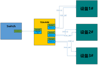
3) TDA4 Serdes0 pairs to Switch, TDA4 uses QSGMII, Switch uses 5GBASE-R. Are the two protocols compatible?
4) Could you help give a EMMC list supported by TDA4VM?
5) Is the clock source internal to pcie0/pcie1/pcie2 the same?
6) MAIN RGMII must be 1.8 V for 1000M operation? Does the 3.3V level support 1000M?
Could you help check this case? Thanks.
Best Regards,
Cherry

