Part Number: SK-TDA4VM
Hi team,
Here're few questions from the customer may need your help:
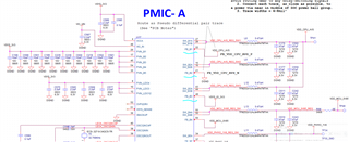
In the above reference design, three SWB1A, SWB2A, SWB3A outputs are combined to one output VDD_CPU_AVS:
1) On P44, it requires FB_B1 and FB_B2 to use a class differential routing, why?
2) On P44, FB_B2 directly connected to DGND, why?
3) On P44, U17 chip FB_B3 is connected to vsys_IO_3V3 which is the output voltage of U27.
Is it for voltage monitoring of vsys_IO_3V3? How does detailed monitoring work and how to turn on this monitoring feature? Is there any documents for reference?
4) On P45, vsys_IO_3V3 connected to FB_B4 of U8 chip and also used for voltage monitoring vsys_IO_3V3.
Is it redundant to repeat the voltage monitoring of vsys_IO_3V3? Or are there any special considerations?
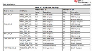
5) The input voltage and output voltage are monitored by the PMIC chip TPS65941. What happens to the PMIC or what is the next action when Vout/Vin exceeds the threshold value?

Could you help check this case? Thanks.
Best Regards,
Cherry


