This thread has been locked.

If you have a related question, please click the "Ask a related question" button in the top right corner. The newly created question will be automatically linked to this question.

DRA821U: DRA821U: UDMA utilize OSPI access NorFlash configure read data length of every read command

Part Number: DRA821U
Other Parts Discussed in Thread: DRA821

Hello,

We are using DRA821 UDMA to load a large mount of code in NorFlash to RAM during the initialization, and we found it took much more time than we expected.

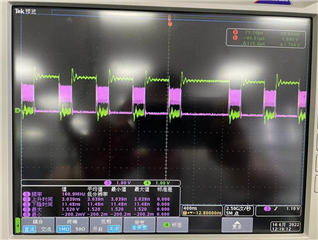
Following is the signals of CS and data line captured by oscilloscope. The green signal is CS, and the purple one is data line. We consult the NorFlash provider(IFX, s28hs512t) that there shall be a minimum interval between every read command called dummy cycles, and as shown in below figure, there are two many dummy cycles which result in low usage of data transformation. In other words, we want to increase the data length of every read command, which can significantly reduce the "idle" time between each read command.

However, we can't find the way to configure it. For UDMA, we can only configure UDMA read total size which the size of whole software code, and the UDMA utilizes OSPI DAC mode to direct access NorFlash.

Do you have any idea how to solve this problem?

Thank you very much!

  • verify udma speed from example "udma_ospi_flash_test", modify udma_ospi_flash_test to change the test receive buffer from TCM memory to DDR, and support 500kB size,  the result is:

    OSPI RCLK running at 166666666 Hz.
    UDMA OSPI Flash application started...

    OSPI Write 1024 bytes in 1040736840ns.
    OSPI Read 1024 bytes in 3675ns.
    OSPI Read 1024 bytes in 3530ns.
    OSPI Read 1024 bytes in 3535ns.
    OSPI Read 1024 bytes in 3525ns.
    OSPI Read 1024 bytes in 3520ns.
    OSPI Read 1024 bytes in 3525ns.
    OSPI Read 1024 bytes in 3520ns.
    OSPI Read 1024 bytes in 3520ns.
    OSPI Read 1024 bytes in 3525ns.
    OSPI Read 1024 bytes in 3520ns.

    Average time for OSPI Read 1024 bytes = 3535ns.


    OSPI flash test at 166MHz RCLK - Read/Write 1024 Bytes have passed

    =====================================

    OSPI RCLK running at 166666666 Hz.
    UDMA OSPI Flash application started...

    OSPI Write 1024 bytes in 1019334075ns.
    OSPI Read 1024 bytes in 4290ns.
    OSPI Read 1024 bytes in 3860ns.
    OSPI Read 1024 bytes in 3860ns.
    OSPI Read 1024 bytes in 3845ns.
    OSPI Read 1024 bytes in 3845ns.
    OSPI Read 1024 bytes in 3845ns.
    OSPI Read 1024 bytes in 3850ns.
    OSPI Read 1024 bytes in 3850ns.
    OSPI Read 1024 bytes in 3845ns.
    OSPI Read 1024 bytes in 3845ns.

    Average time for OSPI Read 1024 bytes = 3890ns.


    OSPI flash test at 166MHz RCLK - Read/Write 1024 Bytes have passed

    OSPI RCLK running at 166666666 Hz.
    UDMA OSPI Flash application started...

    OSPI Write 512000 bytes in 1142566130ns.
    OSPI Read 512000 bytes in 161180ns.
    OSPI Read 512000 bytes in 160640ns.
    OSPI Read 512000 bytes in 160640ns.
    OSPI Read 512000 bytes in 160630ns.
    OSPI Read 512000 bytes in 160635ns.
    OSPI Read 512000 bytes in 160630ns.
    OSPI Read 512000 bytes in 160630ns.
    OSPI Read 512000 bytes in 160630ns.
    OSPI Read 512000 bytes in 160635ns.
    OSPI Read 512000 bytes in 160630ns.

    Average time for OSPI Read 512000 bytes = 160685ns.


    OSPI flash test at 166MHz RCLK - Read/Write 500 KBytes have passed

    -----------------------------------

    please upload you test result to compare the copy speed

  • Can you also please share below details

    • Scope capture for the data with respect to the OSPI clock
    • Which is the code being used for the data transfer. Is it sbl?
    • What is the size of data being transferred from NOR flash to memory and what is the throughput being observed?
  • Zhongyi, 

    can you also provide a register dump of you FSS, and OSPI? We need to check if XIP prefetching is enabled (xipdis=0 in FSS config space) and if PHY pipeline mode is enabled in OSPI. you can ignore the ECC registers. 

    thanks

    Jian

  • Dear all,

    reply as below:

    The driver we use is TI MCAL Fls driver, the configuration as below:

    CONST(struct Fls_ConfigType_s, FLS_CONFIG_DATA) FlsConfigSet =
    {
        .Fls_JobEndNotification = NULL_PTR,
        .Fls_JobErrorNotification = NULL_PTR,
        .maxReadNormalMode = 1024U,
        .maxWriteNormalMode = 256U,
        .sectorList =
        {
                [0] =
                {
                    .numberOfSectors = 256U,
                    .sectorPageSize = 256U,
                    .sectorSize = 262144U,
                    .sectorStartaddress = 1342177280U,
                },
            },
        .dacEnable = TRUE,
        .xipEnable = FALSE,
    #ifdef OSPI_166MHz
        .ospiClkSpeed = 166666666U,
    #else
        .ospiClkSpeed = 133333333U,
    #endif
        .dtrEnable = TRUE,
        .phyEnable = TRUE,
    };
    
    and phy+pipeline mode is used during UDMA transfer.

    • Scope capture for the data with respect to the OSPI clock
      • See below.
    • Which is the code being used for the data transfer. Is it sbl?
      • SBL load App code
    • What is the size of data being transferred from NOR flash to memory and what is the throughput being observed?
      • every transfer size is larger than 1.5M

    For the scope capture, pic1 is the data transfer during one CS pull-down cycle, could you please tell us how many data is transferred?

    there is a lot of potential not fully utilized.

    If we increase the size of transferred data every command(CS(every blue) line pull down cycle),

    the data transfer time can be largely decreased, as seen in pic2

    Thank you !

  • Hello,

    I don't have the experience of dumping FSS register...

    However, the XIP is disabled, and PHY pipeline mode is enabled when we use UDMA to access NorFlash, is this information enough for you?

  • Zhongyi, 

    You can refer 12.3.1.6 FSS Registers and 13.3.2.6.6 OSPI Module Configuration Registers sections in the TRM (https://www.ti.com/lit/ug/spruiu1a/spruiu1a.pdf) for the register address space for getting the register dump.

    Can you please point me to the exact signal which is clock and data in the scope captures you have shared. Both the pictures look like CS vs data.

    The time between two consecutive CS low states is the time gap between two flash read API calls, but not the dummy cycles. Have you tried increasing 'maxReadNormalMode' beyond 1024 in your flash configuration and see if it makes any difference?

    Can you please share the exact flash/udma read API sequence you are calling or point me to the app code you are using?

    - Pratap.

  • Zhongyi/Pratap, 

    On the register dump, the IP owner mentioned to me there may be some mixed up in the TRM about the register addresses. so please read and send back the following address spaces:

    • MCU_FSS0_CFG: 0x0047000000 to 0x00470000FF, 256 B
    • MCU_FSS0_FSAS_CFG:  0x0047010000 to 0x00470100FF, 256 B
    • MCU_FSS0_OSPI0_CTRL: 0x0047040000 to 0x00470400FF, 256 B

    also on the scope shot, can you zoom-in and count how many clock interface cycles when CS is asserted. 

    These are in parallel to Pratap's software debug questions, where we want to review if there is any hardware issues. 

    thanks

    Jian

  • Both the pictures are CS and clock during udma transfer from NorFlash to DDR.

    we are not using any flash read API, they are all from one udma transfer.

    some code listed here:

     Std_ReturnType ReadFlashByUdma(uint32 srcAddr_u32, uint32 destAddr_u32, uint32 size_u32, uint8 idCore_u8)
    {
        uint64 tDest_u64;
        uint32 tLength_u32;
        uint32 q, r;
        uint32 packCnt0_u32;
        uint32 packCnt1_u32;

        Std_ReturnType retVal = E_OK;

        /* enable OSPI to PHY pipeline mode, before DMA transfer */
        CSL_ospiPipelinePhyEnable((const CSL_ospi_flash_cfgRegs *)CSL_MCU_FSS0_OSPI0_CTRL_BASE, TRUE);

        /* for DMA transfer, all address should be SoC memory map */
        tDest_u64 = Memlay_GetGlobalAddress(idCore_u8, destAddr_u32);

        while(size_u32 > 0uL)
        {
            if(size_u32 < 0x10000uL)
            {
                q = 0uL;
                r = size_u32;
            }
            else
            {
                q = size_u32 / MEMLAY_UDMA_1D_MAX_SIZE;
                r = size_u32 % MEMLAY_UDMA_1D_MAX_SIZE;
            }

            if(q > 0uL)
            {
                tLength_u32 = MEMLAY_UDMA_1D_MAX_SIZE;
                size_u32 = r;
            }
            else
            {
                q = 1uL;
                tLength_u32 = r;
                size_u32 = 0uL;
            }

            /* get channel status before transfer */
            (void)Memlay_UdmaGetChPacketCnt(&packCnt0_u32);

            if(E_OK == Memlay_UdmaTrpdInit(tDest_u64, (uint64)srcAddr_u32, (uint16)tLength_u32, (uint16)q))
            {
                tDest_u64 += tLength_u32 * q;
                srcAddr_u32 += tLength_u32 * q;

                /* PRQA S 771 20 */
                do
                {
                    /* completed packet count increases by 1 when finished */
                    (void)Memlay_UdmaGetChPacketCnt(&packCnt1_u32);
                }
                while(packCnt1_u32 == packCnt0_u32);
            }
            else
            {
                retVal = E_NOT_OK;
                break;
            }

            (void)Memlay_UdmaRingFlushRaw();
        }

        return retVal;
    }