This thread has been locked.

If you have a related question, please click the "Ask a related question" button in the top right corner. The newly created question will be automatically linked to this question.

DRA821U: 821 slave SPI

Part Number: DRA821U
Other Parts Discussed in Thread: DRA821, TDA4VM, SYSCONFIG

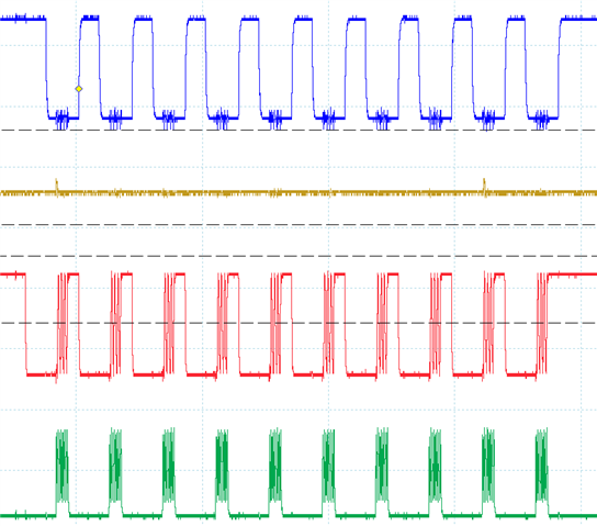
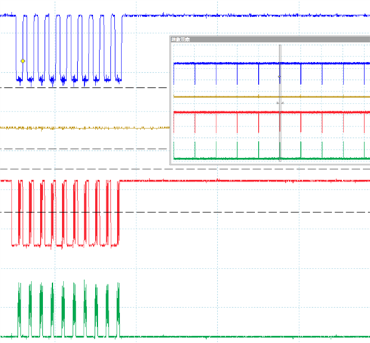
The SPI master/slave communication between 397 and 821 failed.  397 is the master and 821 is the slave.

According to the waveform, 821 did not correctly output the data written in the TX register.

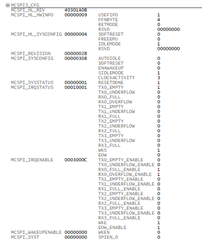
According to the register, 821 SPI RX register has not received data, RX-related interrupt flag bit has not been set.


Here are the configuration details:

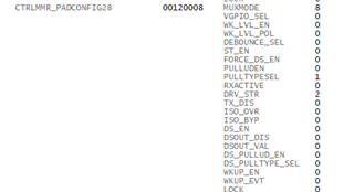
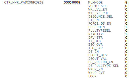
The value of PADCONFIG is set to 0x50008, and the U17 SPI3_D1 CTRLMMR_PADCONFIG28 is set to 0x120008 to enhance the driver strength. However, the output waveform is still incorrect and does not correspond to 0x7777777 written in the TX register.

T14

SPI3

SPI3_CLK

CTRLMMR_PADCONFIG26


U18

SPI3

SPI3_D0

CTRLMMR_PADCONFIG27

DATA INPUT

U17

SPI3

SPI3_D1

CTRLMMR_PADCONFIG28

DATA OUTPUT

U16

SPI3

SPI3_CS0

CTRLMMR_PADCONFIG22


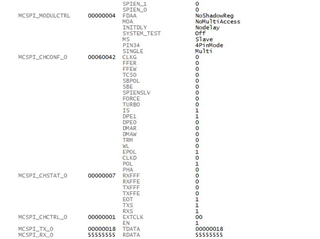
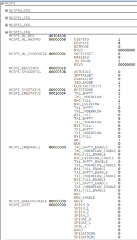
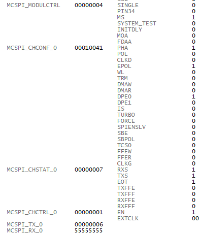
The configuration of SPI3 is as follows:


Question:

  1. Why can't RX register receive a value? Rx-related interrupt flag bit cannot be set
  2. Why write 0x77777777 in TX register, the output waveform is always triangular wave, not 0x 0111 0111
  3. Why does the shift register not work
  • Hi ming li,

    Which driver and which SDK are you using? Can you please provide some more information? 

    Regards,

    Brijesh

  • Thanks for your reply,

     ti-processor-sdk-rtos-j7200-evm-08_02_00_05\pdk_j7200_08_02_00_21\packages\ti\csl\example\mcspi\mcspiMasterSlave\mcspiMasterSlave_spi1_spi2_v1.c

    Since the demo in the SDK cannot meet the requirements, I wrote the SPI slave function with reference to mcspiMasterSlave_spi1_spi2_v1.c and the corresponding underlying code, hoping to realize SPI communication with TC397.

    The basic slave initialization and sending logic are shown in the screenshot.

    I tried sending using both polling/interrupt mode, but neither worked. I think my configuration process can also be seen from the screenshots of the registers above.


    Question:

    1. Why can't RX register receive a value? Rx-related interrupt flag bit cannot be set

    2. Why write 0x77777777 in TX register, the output waveform is always triangular wave, not 0x 0111 0111

    3. Why does the shift register not work

  • Ming, 

    checking your pinmux settings, you mentioned:

    >>CTRLMMR_PADCONFIG28 is set to 0x120008 to enhance the driver strength. 

    why do you set 1 to TX_DIS bit? this bit enabled output buffer of the IO. Also I don't think you need DS_EN either. 

    Please also check your other PADCONFIG registers, where: 

    SPI_CLK should have RX_ACTIVE to accept clock from the master. and, data input pin should have RX_ACTIVE to enable receive buffer of the IO. 

    you may use the pinmux tool to properly configure the interface pins. It will generate the correct settings for you. 

    also if you get chance to capture the waveform again, please have one screenshot of zoomed-in SPI_CLK, so we can see if the clk sent from the master looks okay. in your original diagram, it is too small to see. 

    thanks

    Jian

  • i did not set TX_DIS bit and DS_EN ,please answer my question:

    1. Why can't RX register receive a value? Rx-related interrupt flag bit cannot be set

    2. Why write 0x77777777 in TX register, the output waveform is always triangular wave, not 0x 0111 0111

    3. Why does the shift register not work

  • Hi Ming,

    Referring to the waveform in the original post, can you check why chip select line is toggling like this? This might be causing the above issues. The CS line should remain low for a given transaction, something like as the waveform below:

    Regards,
    Parth

  • The current situation:

    TDA4 serves as 397's slave
    The master sends 0x55555555, the RX register can receive the value, but the value written by the TX register cannot be output on the pin.

    821 serves as the slave of 397
    The master sent 0x55555555, 821 cannot receive the data from 397, nor can it send the data from the TX register.

    Basically, the slave program is the same for both chips.

    TDA4 :Why the value written in the TX register did  not sent out?

    dra821:   why TX RX dont work? 

  • Hi Ming,

    Can you share the waveform captured with TDA4VM? Also, did you get a chance to look into why CS line is toggling?

    Regards,
    Parth

  • Hi, Jian,

    I am looking into this issues with UAES. And I have test MCSPI_Slave_TestApp and csl_mcspi_masterslave_app on EVM, both succeed. However because  MCSPI demo in PDK are concerned about MCU_SPI2 and MAIN_SPI4, which are connected internally. So we can not get the standard parameters of pad config. Could you provide recommended pad config parameters.  

    Thanks.

  • Zekun, 

    below is the generated SPI3 file from sysconfig:

    https://dev.ti.com/sysconfig/?fromPinmux=true#/config/?args=--device%20J7200_DRA821_SR1.0_alpha%20--part%20Default%20--package%20ALM%20--theme%20light

    where i set D0 as input and D1 as output. I did not get a chance to check yet, though the tool has been extensively used for PDK and linux pinmux configurations.

    Jian 

    static pinmuxPerCfg_t gSpi3PinCfg[] =
    {
        /* MySPI3 -> SPI3_CLK -> T14 */
        {
            PIN_MCAN9_TX, PIN_MODE(8) | \
            ((PIN_PULL_DISABLE | PIN_INPUT_ENABLE) & (~PIN_PULL_DIRECTION))
        },
        /* MySPI3 -> SPI3_D0 -> U18 */
        {
            PIN_MCAN9_RX, PIN_MODE(8) | \
            ((PIN_PULL_DISABLE | PIN_INPUT_ENABLE) & (~PIN_PULL_DIRECTION))
        },
        /* MySPI3 -> SPI3_D1 -> U17 */
        {
            PIN_MCAN10_TX, PIN_MODE(8) | \
            ((PIN_PULL_DISABLE) & (~PIN_PULL_DIRECTION & ~PIN_INPUT_ENABLE))
        },
        /* MySPI3 -> SPI3_CS0 -> U16 */
        {
            PIN_MCAN7_TX, PIN_MODE(8) | \
            ((PIN_PULL_DISABLE | PIN_INPUT_ENABLE) & (~PIN_PULL_DIRECTION))
        },
        {PINMUX_END}
    };

  • Based on the application scenario, I set SPI slave D0 as input and D1 as output. For the case of SPI as slave, will this cause the value written in the TX register can not be sent from D1?

  • Ming, this configuration have no effect to TX sending from D1. We will go on debugging. 

  • As discussed within TI team:

    1. Ming to post updated scope shots for SPI3_D1 pin. 

    2. Ming to send updated CTRLMMR_PADCONFIG28 driver. 

    3. Jian to confirm difference of CSL and driver example in PDK. 

    we would like to probe if the issue is related to pin configuration or driver. 

    Jian

  •       help UAES to upload these images. Please help to analyze these info.

  • thanks to zekun.bai, By setting the WL bit and CTRLMMR_SPI3_CLKSEL, the 821 can communicate with the TC397, and I am currently testing the SPI communication between the TDA4 and the 397.