This thread has been locked.
If you have a related question, please click the "Ask a related question" button in the top right corner. The newly created question will be automatically linked to this question.

Hi Peter,
The VC5509A bootloader is described here: https://www.ti.com/lit/pdf/spra375. Please see 2.3.6 I2C EEPROM-Boot Mode for details on I2C boot mode.
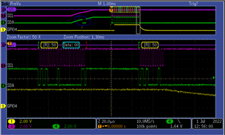
Looking at your scope captures, I'm having trouble differentiating the passing and failing test cases. What is different between the two?
Do you see the pattern described in "Figure 8. Reading the First Byte in a 64Kbyte Block" for the passing case?
What do you see with respect to this pattern in the failing case?
There is limited support on this device and I wanted to share the support guidance for this device also here: https://e2e.ti.com/support/processors-group/processors/f/processors-forum/818771/faq-support-guidance-for-c5000-digital-signal-processors
I've looped in a colleague in case further comment is required.
Regards,
Frank
Thanks Frank. In the second image, where it passes, the DSP clocks SDA enough to get address (50) and data (00) and after a pause, GPIO4 tristates. In the first image, where it fails, the DSP stops clocking after the address (50). This leaves SDA low, which usually isn't good on an i2c bus. It also seems interesting that GPIO4 appears to tristate here, during the i2c exchange. Is there an unexpected state change in the boot loader stranding SDA low? I am familiar with SPRA375. Following the troubleshooting in that document in section 3.6:
GPIO4 does go low at the start.
Does GPIO4 "toggle during the random read"? It does go from low to high. Is that enough? I think so since the pass and fail cases have the same number of toggles.
I don't think the last two troubleshooting points apply since the DSP never loads code from the EEPROM and thus never gets to code execution.
Our CLKIN is 12MHz, which is within spec, but at the high end of the range. I don't see anything else in the documentation to suggest any other fixes or best practices. What would you suggest?
Hi Peter,
In the second image, where it passes, the DSP clocks SDA enough to get address (50) and data (00) and after a pause, GPIO4 tristates. In the first image, where it fails, the DSP stops clocking after the address (50)
According to SPRA375:
The I2C boot process begins with the DSP using a random read command to read address zero of the
EEPROM. A random read command, as shown in Figure 8, consists of a dummy write command with the
address set to zero, immediately followed by a current address read command. The EEPROM responds
by sending a data byte to the DSP. The DSP depends on the ability of the EEPROM to automatically
increment the address internally to read the subsequent bytes. All subsequent bytes are read using the
current address read command as shown in Figure 9.
The bootloader flags the start of I2C-boot mode by setting the GPIO4 low during the random read
operation. The GPIO4 is then set high during the rest of the read operations. The I2c module remains
enabled (but no bus activities) at the end of the boot process, until the user's application turns the module
off.
I see this behavior in the third scope capture, but not the first two. The third capture also seems to show correct behavior for GPIO4, i.e. low during random read and high afterwards.
The first two scope captures (first:failing, second:passing) don't seem to show the expected pattern. What are these I2C transactions doing? These appear to be read commands. Are these the first transaction you observe after POR?
the DSP stops clocking after the address (50)
The DSP stops clocking SCL? Is the read a full I2C transaction? Which device (DSP or EEPROM) is driving SDA low?
For the failing case, I notice some kind of glitch on the SDA line before the first transacation. What is this? Does this alway occur in the failing case?
Our CLKIN is 12MHz, which is within spec, but at the high end of the range.
Have you tried reducing the frequency?
I don't see anything else in the documentation to suggest any other fixes or best practices. What would you suggest?
Unfortunately, I don't have access to the bootloader source code or an EVM with this device. Given the information you've shared, I would suspect some intermittent hardware issue. Have you tried replacing the EEPROM in one of the failing boards?
I've looped in another colleague for further comment.
Regards,
Frank
Frank,
The 2nd and 3rd captures are essentially one and the same, the 3rd capture just has a much longer timescale. The 2nd capture shows the first burst of activity on the i2c bus. This corresponds with the trigger point on the far left of the 3rd capture. The zoomed in portion of the 3rd capture shows the start of the second burst of activity, roughly 550ms after the first burst. It looks like the 2nd burst of activity (shown in the 3rd capture above) shows the address incrementing as the DSP reads from the EEPROM and shows proper random read command behavior as you point out from SPRA375 and figure 8.
I've marked up captures 2 & 3 to illustrate their relation:

As for what the first two captures show (i.e. the initial burst of activity on the i2c bus) I was hoping you could tell me. I have no idea what the DSP is trying to accomplish here.
The DSP is the only driver of SCL, so yes, my assertion is that the DSP stops clocking SCL in capture 1. The read does not appear to be a full i2c transaction since in the passing case the DSP will keep clocking in order to drive the read command to completion as shown in capture 2. This doesn't happen in capture 1. I would assume the EEPROM is driving SDA low. See the passing scenario. The DSP has just issued a read command so the EEPROM does what it's been asked to do. Only problem is, in the fail case, the DSP never completes the command. In fact, the DSP never does anything after this.
I haven't ran this test enough to know if the glitch on SDA is present in every fail case and absent in every pass case. This is during the period when +3.3V is ramping up. Again, I don't know what this is but perhaps there's a clue since we see a GPIO4 pulse here as well, in both cases.
I have not tried reducing the frequency, but there might be some merit to the idea.
I have not tried swapping the EEPROM. I don't really suspect it as it seems to be responding properly to the commands the DSP is giving it.
It seems I've failed to mention this: To capture the fail scenario, I'm heating the DSP up to around 50C. At room temp, it passes every time. Warmed up, it fails consistently.
Peter
Hi Peter,
To capture the fail scenario, I'm heating the DSP up to around 50C. At room temp, it passes every time. Warmed up, it fails consistently.
Thanks for sharing this additional information. The seems like an important observation. To me, this suggests a hardware issue. Hence, I'm reassigning this thread to a HW expert.
I want to reiterate the point I made above:
There is limited support on this device and I wanted to share the support guidance for this device also here: https://e2e.ti.com/support/processors-group/processors/f/processors-forum/818771/faq-support-guidance-for-c5000-digital-signal-processors
Regards,
Frank
Hi Peter,
If heating the boards has some impact on the behavior, have you tried looking at the solder reflow quality? Is it possible there is either a poor solder joint, or an excess solder blob or similar that is changing the physical connections on the boards during high temp? Also, you could try just reflowing the entire board (or the area around the DSP and the I2C memory).
Another thing you could do is cut the SDA trace between the pullup resistor and the I2C memory and solder down a small resistor (something like 100ohms would be fine). Then when you scope the the bus (making sure to do so at the pullup resistor), you can look at the actual voltage level of a "low" to determine which device is holding the line low. If the resistor is placed between the pullup and the I2C memory as described above, you will see true 0.0V when the C5000 pulls SDA low, and around 63mV when the I2C memory is holding SDA low.
Looking at the waveforms, it appears something is holding SDA low following the ACK of the address and r/w bit transaction. Identifying which device is holding it low may be helpful for determining what is causing the problem.
Thanks,
Mike