This thread has been locked.

If you have a related question, please click the "Ask a related question" button in the top right corner. The newly created question will be automatically linked to this question.

TDA4VM: DCC(Dual Clock Comparator) module inside the TDA4

Part Number: TDA4VM

hi experts,

   I'm trying to understand the default code of DCC inside the SDL package, the folder as : SDL_1.0/SDL_RLS_01.00.00/sdl/examples/dcc/UC8.

   the Source clock is RC OSC and Test clock is HFOSC0, I also can understand the HFOSC0 is 19200(19.2MHZ), but what's the RC OSC clock? I see it's 333334 in the code, But I only can see it’s 12.5MHZ in the TRM, could you please guide us what's this and is it related with the HW? 
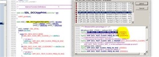
 

   and also, why we choose this clock 333334 as input, is it determined by HW connection?
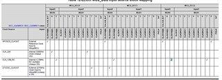
  

   thanks in advance.

Br,

Neo

  • Hi Neo,

    As per the Safety Manual, the DCC is a diagnostic mechanism that can be used to detect clocking issues, including incorrect frequency and drift between clock sources.  The DCC measures the frequency of a selectable clock source using another input clock as reference. Both reference clock and clock under test may be selected via software, as can the expected ratio of clock frequencies.

    In regards to UC8, looks like there is an issue with the code, which I am following up internally.

    Looking at the code of UC8

    • Input0 the reference clock is set to SDL_DCC_CLK0_SRC_CLOCK0_2, 
    • Input1 the test clock is set to SDL_DCC_CLK1_SRC_CLOCKSRC7.

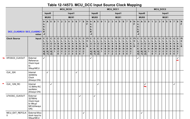
    Based on the TRM, and matching the variable naming to the below table, one would then expect the below settings to be in use:

    • Input 0 = CLK_12M_RC
    • Input 1 = HFOSC0_CLKOUT

    Which would have frequencies of:

    • CLK_12M_RC = 12.5 Mhz
    • HFSOSC0_CLKUT = 19.2 Mhz

    And aligns with the comments in the code for UC8,where

    • Module instance MCU_DCC2 is being used
    • RC OSC0 is the reference clock being used
    • HFOSC0 is the clock under test. 

    What does not match is:

    • The code in main.h where, 333334 Khz is being used as the expected input for  the clock under test.

    So how is the test case passing? 

    • The comments in main.c indicate MCU_DCC2 is under test, (which is what APP_DCC_MODULE_INST is set to), but further below, in step 4, SDL_DCC_INST_MCU_DCC0 is being configured

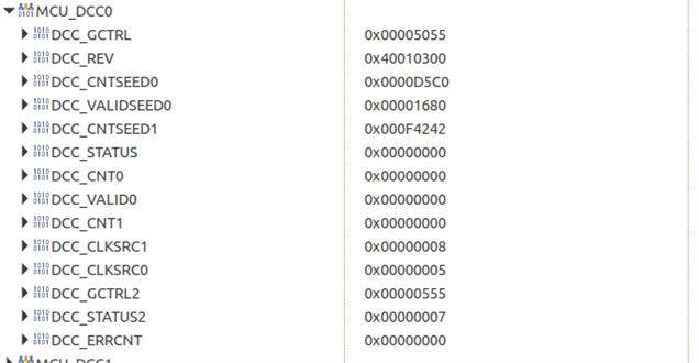
    When running UC8, which CCS the CLKSRC's for MCU_DCC0 can be seen to be set as below.

    Which matches the code in Step 4, where MCU_DCC0 is being configured.

    After configuration of MCU_DCC0, the MCU_DCC2 interrupts are enabled

    As MCU_DCC0 runs for it's allotted time period, and passes, as no interrupts go off.

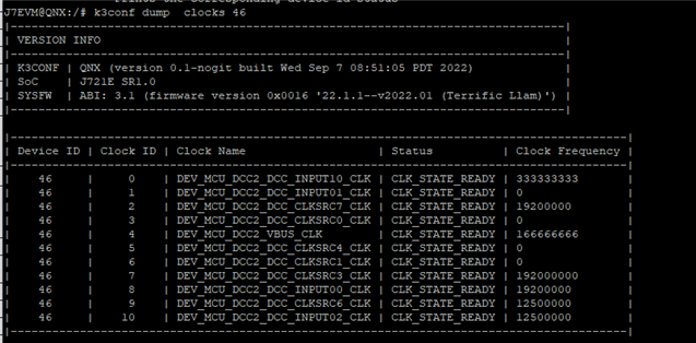
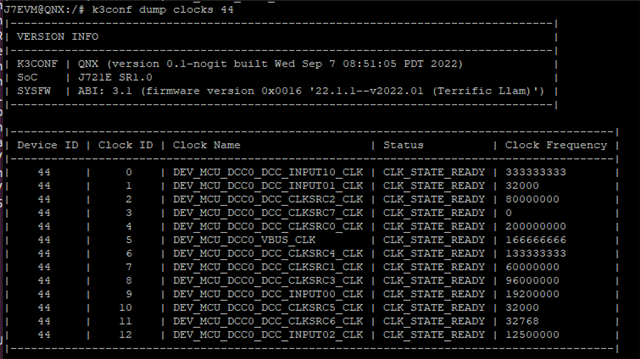
    Below is what the clocks look like for MCU_DCC2 and MCU_DCC0 when viewed by k3conf from A72.

    Regards,

    Kip

  • Hi Neo,

    My understanding is that a patch has already been provided to you for this issue, which is covered by [PROC_SDL-3701] DCC: Value to select Input0 clock other than clock0_0 is not correct - Texas Instruments JIRA.

    Closing this thread.

    Regards,

    Kip