This thread has been locked.

If you have a related question, please click the "Ask a related question" button in the top right corner. The newly created question will be automatically linked to this question.

TDA4VM: J721S2 Dual Comparator Clock

Part Number: TDA4VM

Hi Experts,

I am trying to figure out how to connect some of the clocks to set up the J721S2 Dual Clock Comparators.


The J721E chip has 13 DCCs while the J721S2 has only 10.


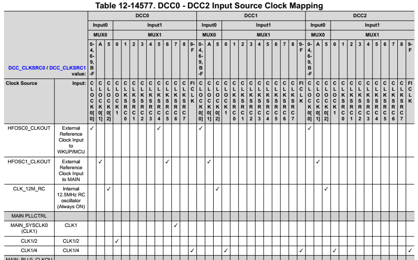
Looking at table 12-14577 in the J721E TRM (was unable to find in J721S2 TRM) I was able to get one instance to work correctly in single shot mode. MAIN DCC1, MAIN_PLL1_HSDIV6_CLKOUT (19.2MHz) and CLK_12M_RC (12.5MHz).
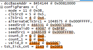
I have tried various combinations in other DCCs and the DCC has an error status before starting to count down the counters.

The values seem correct in the configuration struct but doesn’t work as expected.


Do the DCCs for the J721S2 line up with DCC 0-9 in table 12-14577 in the TRM or is it a different table matrix?

  • Please search for DCC in TRM section Device Configuration -> Clocking -> Clock Mapping.

  • Thanks for the information. The table was is taken from a fairly old version of the TRM (December 2020). I see looking at newer versions for both J721E and J721S2 these tables were removed. The section this was in was 12.11.1.2 DCC Integration.

    Is see how the tables in clock mapping line up to the old version and can now move forward with testing.

    Thanks!

  • Is this helpful?

    MAIN_DCC_0 MAIN_DCC_1 MAIN_DCC_2 MAIN_DCC_3 MAIN_DCC_4 MAIN_DCC_5 MAIN_DCC_6 MAIN_DCC_7 MAIN_DCC_8 MAIN_DCC_9 MCU_DCC_0 MCU_DCC_1 MCU_DCC_2
    Clock Divider Clock Divider Clock Divider Clock Divider Clock Divider Clock Divider Clock Divider Clock Divider Clock Divider Clock Divider Clock Divider Clock Divider Clock Divider
    CLKSRC0 postdiv3_16fft.main_0.hsdivout8_clk 1 postdiv3_16fft.main_0.hsdivout5_clk 1 postdiv3_16fft.main_1.hsdivout7_clk 1 hsdiv2_16fft.main_4.hsdivout0_clk 1 hsdiv4_16fft.main_0.hsdivout1_clk 2 1 MCASP0_ACLKX.MCASP0_ACLKX 1 AUDIO_EXT_REFCLK0.AUDIO_EXT_REFCLK0 1 j7am_wakeup_16ff.wkup_0.wkup_rcosc_32k_clk 1 hsdiv4_16fft.main_3.hsdivout3_clk 1 hsdiv4_16fft.mcu_1.hsdivout0_clk 2 hsdiv4_16fft.mcu_2.hsdivout1_clk 2 MCU_RMII1_REF_CLK.MCU_RMII1_REF_CLK 1
    CLKSRC1 hsdiv4_16fft.main_0.hsdivout2_clk 1 postdiv3_16fft.main_0.hsdivout6_clk 1 postdiv3_16fft.main_1.hsdivout8_clk 1 hsdiv1_16fft.main_5.hsdivout0_clk 2 1 hsdiv1_16fft.main_19.hsdivout0_clk 2 MCASP0_ACLKR.MCASP0_ACLKR 1 AUDIO_EXT_REFCLK1.AUDIO_EXT_REFCLK1 1 LPXOSC.CLKOUT 1 hsdiv4_16fft.main_3.hsdivout4_clk 1 hsdiv4_16fft.mcu_1.hsdivout1_clk 1 hsdiv4_16fft.mcu_2.hsdivout2_clk 1 MCU_RGMII1_RXC.MCU_RGMII1_RXC 1
    CLKSRC2 hsdiv4_16fft.main_0.hsdivout3_clk 1 postdiv3_16fft.main_0.hsdivout7_clk 1 1 hsdiv1_16fft.main_5.hsdivout1_clk 2 hsdiv0_16fft.main_12.hsdivout0_clk 4 hsdiv1_16fft.main_17.hsdivout0_clk 2 MCASP1_ACLKX.MCASP1_ACLKX 1 hsdiv2_16fft.main_14.hsdivout2_clk 4 MCU_EXT_REFCLK0.MCU_EXT_REFCLK0 1 RMII_REF_CLK.RMII_REF_CLK 1 hsdiv4_16fft.mcu_1.hsdivout2_clk 1 hsdiv4_16fft.mcu_2.hsdivout3_clk 1 HFOSC1.CLKOUT 1
    CLKSRC3 hsdiv4_16fft.main_0.hsdivout4_clk 1 hsdiv4_16fft.main_1.hsdivout0_clk 1 hsdiv4_16fft.main_2.hsdivout4_clk 1 4 hsdiv0_16fft.main_26.hsdivout0_clk 4 hsdiv1_16fft.main_25.hsdivout0_clk 2 MCASP1_ACLKR.MCASP1_ACLKR 1 1 K3_DPHY_RX.main_0.ppi_rx_byte_clk 1 mcasp.main_4.mcasp_ahclkr_pout.0 1 hsdiv4_16fft.mcu_1.hsdivout3_clk 1 hsdiv4_16fft.mcu_2.hsdivout4_clk 1 postdiv3_16fft.main_1.hsdivout5_clk 1
    CLKSRC4 HFOSC0_CLOCKLOSS_DETECTION.HFOSC0_CLKOUT 1 hsdiv4_16fft.main_1.hsdivout1_clk 1 postdiv2_16fft.main_2.hsdivout6_clk 1 1 hsdiv2_16fft.main_14.hsdivout0_clk 4 hsdiv1_16fft.main_25.hsdivout1_clk 2 MCASP2_ACLKX.MCASP2_ACLKX 1 1 K3_DPHY_RX.main_1.ppi_rx_byte_clk 1 RGMII1_RXC.RGMII1_RXC 1 hsdiv4_16fft.mcu_1.hsdivout4_clk 1 hsdiv1_16fft.mcu_0.hsdivout0_clk 4 MCU_OSPI1_LBCLKO.MCU_OSPI1_LBCLKO 1
    CLKSRC5 HFOSC1.CLKOUT 1 hsdiv4_16fft.main_1.hsdivout2_clk 1 hsdiv4_16fft.main_2.hsdivout1_clk 2 hsdiv0_16fft.main_6.hsdivout0_clk 4 hsdiv2_16fft.main_14.hsdivout1_clk 4 1 MCASP2_ACLKR.MCASP2_ACLKR 1 VOUT0_EXTPCLKIN.VOUT0_EXTPCLKIN 1 hsdiv2_16fft.main_4.hsdivout1_clk 1 j7am_wakeup_16ff.wkup_0.wkup_rcosc_32k_clk 1 hsdiv1_16fft.mcu_0.hsdivout1_clk 1 1
    CLKSRC6 k3_pll_ctrl_wrap.main_0.chip_div1_clk_clk 1 hsdiv4_16fft.main_1.hsdivout3_clk 1 hsdiv4_16fft.main_2.hsdivout2_clk 1 hsdiv0_16fft.main_7.hsdivout0_clk 4 4 GPMC0_CLK.GPMC0_CLK 1 MCASP3_ACLKX.MCASP3_ACLKX 1 postdiv2_16fft.main_2.hsdivout7_clk 1 hsdiv4_16fft.main_3.hsdivout1_clk 1 hsdiv2_16fft.main_4.hsdivout2_clk 1 LPXOSC.CLKOUT 1 MCU_OSPI0_LBCLKO.MCU_OSPI0_LBCLKO 1 RCOSC.CLKOUT 1
    CLKSRC7 eDP_ln0_txclk_div2.out0 1 postdiv3_16fft.main_1.hsdivout6_clk 1 hsdiv4_16fft.main_3.hsdivout0_clk 1 hsdiv0_16fft.main_8.hsdivout0_clk 4 hsdiv1_16fft.main_16.hsdivout0_clk 2 mcasp.main_4.mcasp_ahclkx_pout.0 1 MCASP3_ACLKR.MCASP3_ACLKR 1 CPTS0_RFT_CLK.CPTS0_RFT_CLK 1 hsdiv4_16fft.main_3.hsdivout2_clk 1 1 MCU_EXT_REFCLK0.MCU_EXT_REFCLK0 1 CPSW2G_CPTS_RCLK_SEL.out0 1 HFOSC0_CLOCKLOSS_DETECTION.HFOSC0_CLKOUT 1
    INPUT00 HFOSC0_CLOCKLOSS_DETECTION.HFOSC0_CLKOUT 1 HFOSC0_CLOCKLOSS_DETECTION.HFOSC0_CLKOUT 1 HFOSC0_CLOCKLOSS_DETECTION.HFOSC0_CLKOUT 1 HFOSC0_CLOCKLOSS_DETECTION.HFOSC0_CLKOUT 1 HFOSC0_CLOCKLOSS_DETECTION.HFOSC0_CLKOUT 1 HFOSC0_CLOCKLOSS_DETECTION.HFOSC0_CLKOUT 1 HFOSC0_CLOCKLOSS_DETECTION.HFOSC0_CLKOUT 1 HFOSC0_CLOCKLOSS_DETECTION.HFOSC0_CLKOUT 1 HFOSC0_CLOCKLOSS_DETECTION.HFOSC0_CLKOUT 1 HFOSC0_CLOCKLOSS_DETECTION.HFOSC0_CLKOUT 1 HFOSC0_CLOCKLOSS_DETECTION.HFOSC0_CLKOUT 1 HFOSC0_CLOCKLOSS_DETECTION.HFOSC0_CLKOUT 1 HFOSC0_CLOCKLOSS_DETECTION.HFOSC0_CLKOUT 1
    INPUT01 HFOSC1.CLKOUT 1 HFOSC1.CLKOUT 1 HFOSC1.CLKOUT 1 HFOSC1.CLKOUT 1 HFOSC1.CLKOUT 1 HFOSC1.CLKOUT 1 HFOSC1.CLKOUT 1 HFOSC1.CLKOUT 1 HFOSC1.CLKOUT 1 HFOSC1.CLKOUT 1 j7am_wakeup_16ff.wkup_0.wkup_rcosc_32k_clk 1 LPXOSC.CLKOUT 1 MCU_EXT_REFCLK0.MCU_EXT_REFCLK0 1
    INPUT02 RCOSC.CLKOUT 1 RCOSC.CLKOUT 1 RCOSC.CLKOUT 1 RCOSC.CLKOUT 1 RCOSC.CLKOUT 1 RCOSC.CLKOUT 1 RCOSC.CLKOUT 1 RCOSC.CLKOUT 1 RCOSC.CLKOUT 1 RCOSC.CLKOUT 1 RCOSC.CLKOUT 1 RCOSC.CLKOUT 1 RCOSC.CLKOUT 1
    INPUT10 k3_pll_ctrl_wrap.main_0.chip_div1_clk_clk 2 k3_pll_ctrl_wrap.main_0.chip_div1_clk_clk 4 k3_pll_ctrl_wrap.main_0.chip_div1_clk_clk 4 k3_pll_ctrl_wrap.main_0.chip_div1_clk_clk 4 k3_pll_ctrl_wrap.main_0.chip_div1_clk_clk 2 k3_pll_ctrl_wrap.main_0.chip_div1_clk_clk 1 k3_pll_ctrl_wrap.main_0.chip_div1_clk_clk 4 k3_pll_ctrl_wrap.main_0.chip_div1_clk_clk 2 k3_pll_ctrl_wrap.main_0.chip_div1_clk_clk 2 k3_pll_ctrl_wrap.main_0.chip_div1_clk_clk 2 POST CLK MUX.out0 3 hsdiv4_16fft.mcu_2.hsdivout0_clk 1 POST CLK MUX.out0 3
    VBUSCLK k3_pll_ctrl_wrap.main_0.chip_div1_clk_clk 4 k3_pll_ctrl_wrap.main_0.chip_div1_clk_clk 4 k3_pll_ctrl_wrap.main_0.chip_div1_clk_clk 4 k3_pll_ctrl_wrap.main_0.chip_div1_clk_clk 4 k3_pll_ctrl_wrap.main_0.chip_div1_clk_clk 4 k3_pll_ctrl_wrap.main_0.chip_div1_clk_clk 4 k3_pll_ctrl_wrap.main_0.chip_div1_clk_clk 4 k3_pll_ctrl_wrap.main_0.chip_div1_clk_clk 4 k3_pll_ctrl_wrap.main_0.chip_div1_clk_clk 4 k3_pll_ctrl_wrap.main_0.chip_div1_clk_clk 4 POST CLK MUX.out0 6 POST CLK MUX.out0 6 POST CLK MUX.out0 6
  • This was very helpful. On additional oddity I see is that many of the CLKSRC's seem to have an additional /10 implemented for the DCC.

    For instance, PLL26 HSDIV0 (DDR1) is set to 1066MHz. This lines up with DCC4, CLKSRC3 with a /4 divider which should be reading at 267MHz.

    Testing this for the DCC ended up failing and checking the counts they were going down, but only about 10%. I then tested 26.7MHz and it passed. Is this expected? I am seeing this /10 on quite a few of the other CLKSRCs as well.

    One additional question, I am testing the same thing above with the PLL12 HSDIV0 (DDR0) and the counts for the clksrc never start even though it is enabled as well. Any thoughts why this DCC clock may not be working?

    I have only been testing in single shot mode so far.

  • David,

    Try this (and I'm sorry that it wasn't clearer before):

    1.) INPUT00, INPUT 01, and INPUT 02 are mapped  in register DCC_CLKSRC0 (0, 1, 2) as you would expect.

    2.) INPUT10 is mapped as an input clock in register DCC_CLKSRC1 source 0; and this mapping is not at all clear and NOT as you might expect

    3.) CLKSRC0 -- CLKSRC7 are clock inputs mapped by DCC_CLKSRC1 with a source +1 from their title; so CLKSRC0 is actually DCC_CLKSRC1, source 0+1; CLKSRC2 is mapped by DCC_CLKSRC1, source 2+1...

    4) VBUSCLK can be mapped by DCC_CLKSRC1, source 9 and above.

    If this is not clear enough, please follow-up.

    Kevin

  • Thanks for the clarity, the test I thought I was running for DDR1 was running for DDR0 and now both are running as expected.

    I am still seeing the divide by 10 on the DDR timing. Here is the read of DDR1 testing after completion with a success.

    INPUT 02 is used as the reference and runs at 12.5MHz.
    You can see the ratio of the two seed values is ( 1048575/( 466331 * ~1.05 (drift) ) ) = 2.14

    12.5MHz * 2.14 = 26.7MHz.

    I just tested with INPUT 00 which is at 19.2MHz and changed the frequency of the DDR clocks to 267000MHz and it works.

    The frequency of INPUT 02 must be 125MHz then, but not totally sure that makes sense? INPUT 01 is also passing at 125MHz.

  • David,

    The value of "5" in CLKSRC0 is confusing to me. I would have thought that you'd want it to be 0x2 if you were selecting the 12.5MHz internal oscillator.

    Kevin

  • David,

    Maybe a little fuller explanation -- I think when you have 0x5 for the DCC_CLKSRC0, you are selecting the VBUS_CLK. 

    I tested this for DCC_CLKSRC0 = 0x3 and DCC_CLKSRC = 0x5; in both cases, the clock is coming from VBUS_CLK.

    Kevin

  • Thanks Kevin, that answered it. I was still using the const variables from the example code which matches the CLKSRC0 (0) CLKSRC1 (0xA) CLKSRC2 (0x5) shown in the table 12-14577 that Brad posted above. I understand your comment earlier now better.