Part Number: TDA4VM
Other Parts Discussed in Thread: SYSCONFIG

the sdk version is 07_03_00_07
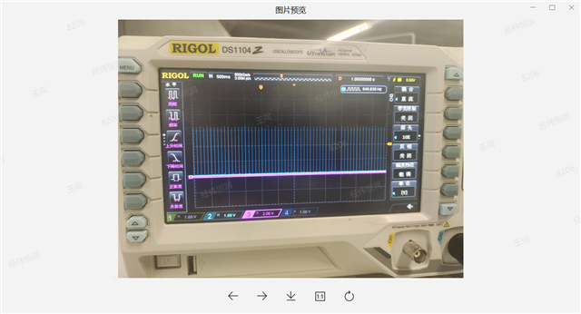
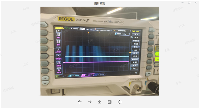
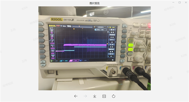
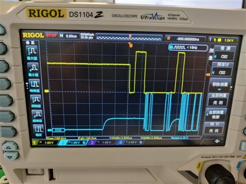
as the image show , we find when the spi in idle state, the MCU_SPI0_SDO single should be low level, but in fact, it is middle level neither high nor low, so why does this happen.
Another question, after the MCU_SPI0_CS being pulled down, the MCU_SPI0_SDO maybe take a long time for the data signal to appear, so whether this phenomenon is normal
here is the spi code, Please help to check whether there is any configuration problem
#include <ti/board/board.h>
#include <ti/board/src/j721e_evm/include/board_pinmux.h>
#include "FS85_Driver.h"
#include <ti/csl/cslr_gtc.h>
#include <ti/board/src/j721e_evm/include/board_pll.h>
#include "sbl_main.h"
#define Log_d(fmt, ...) SBL_log(SBL_LOG_MAX,fmt, ##__VA_ARGS__)
#define Log_i(fmt, ...) SBL_log(SBL_LOG_MAX,fmt, ##__VA_ARGS__)
#define Log_w(fmt, ...) SBL_log(SBL_LOG_MAX,fmt, ##__VA_ARGS__)
#define Log_e(fmt, ...) SBL_log(SBL_LOG_MAX,fmt, ##__VA_ARGS__)
SPI_Handle spi_fs85;
static pinmuxPerCfg_t gMcu_spi0PinCfg[] =
{
/* MyMCU_SPI1 -> MCU_SPI0_CLK -> E27 */
{
PIN_MCU_SPI0_CLK, PIN_MODE(0) | \
((PIN_PULL_DISABLE) & (~PIN_PULL_DIRECTION & ~PIN_INPUT_ENABLE))
},
/* MyMCU_SPI1 -> MCU_SPI0_D0 -> E24 */
{
PIN_MCU_SPI0_D0, PIN_MODE(0) | \
((PIN_PULL_DISABLE) & (~PIN_PULL_DIRECTION & ~PIN_INPUT_ENABLE))
},
/* MyMCU_SPI1 -> MCU_SPI0_D1 -> E28 */
{
PIN_MCU_SPI0_D1, PIN_MODE(0) | \
((PIN_PULL_DISABLE | PIN_INPUT_ENABLE) & (~PIN_PULL_DIRECTION))
},
/* MyMCU_SPI1 -> MCU_SPI0_CS0 -> E25 */
{
PIN_MCU_SPI0_CS0, PIN_MODE(0) | \
((PIN_PULL_DISABLE) & (~PIN_PULL_DIRECTION & ~PIN_INPUT_ENABLE))
},
{PINMUX_END}
};
static pinmuxModuleCfg_t gMcu_spiPinCfg[] =
{
{0, TRUE, gMcu_spi0PinCfg},
{PINMUX_END}
};
static pinmuxBoardCfg_t gJ721E_spiWkupPinmuxData[] =
{
{0, gMcu_spiPinCfg},
{PINMUX_END}
};
static void SPI_InitConfigDefault(SPI_HWAttrs *cfg, uint32_t chn)
{
cfg->chNum = chn;
cfg->chnCfg[chn].tcs = MCSPI_CS_TCS_0PNT5_CLK;
cfg->chnCfg[chn].dataLineCommMode = MCSPI_DATA_LINE_COMM_MODE_6;
cfg->chnCfg[chn].trMode = MCSPI_TX_RX_MODE;
cfg->initDelay = MCSPI_INITDLY_0;
cfg->rxTrigLvl = MCSPI_RX_TX_FIFO_SIZE;
cfg->txTrigLvl = MCSPI_RX_TX_FIFO_SIZE;
}
static void SPI_InitConfig(uint32_t instance, uint32_t chn)
{
SPI_HWAttrs spi_cfg;
/* Get the default SPI init configurations */
SPI_socGetInitCfg(instance, &spi_cfg);
/* Set the default SPI init configurations */
SPI_InitConfigDefault(&spi_cfg, chn);
spi_cfg.baseAddr = CSL_MCU_MCSPI0_CFG_BASE;
/* interrupt enabled */
spi_cfg.enableIntr = false;
spi_cfg.edmaHandle = NULL;
spi_cfg.dmaMode = FALSE;
spi_cfg.inputClkFreq = 20000000U;
// Log_i("error [debug] spi_cfg->baseAddr=0x%x,intNum=%u\n", spi_cfg.baseAddr, spi_cfg.intNum);
/* Transmit/Receive mode */
spi_cfg.chnCfg[chn].trMode = MCSPI_TX_RX_MODE;
/* Set Pin direction */
/* Data line 1 TX enabled, data line 0 RX enabled TX disabled --> MCSPI_DATA_LINE_COMM_MODE_1*/
/* Data line 0 TX enabled, data line 1 RX enabled TX disabled --> MCSPI_DATA_LINE_COMM_MODE_6*/
spi_cfg.chnCfg[chn].dataLineCommMode = MCSPI_DATA_LINE_COMM_MODE_6;
/* Set the SPI init configurations */
SPI_socSetInitCfg(instance, &spi_cfg);
}
int sbl_mian_spi_init(void)
{
int ret = 0;
uint32_t instance;
Board_pinmuxUpdate(gJ721E_spiWkupPinmuxData, 1);
SPI_init();
instance = 0;
SPI_InitConfig(instance, 0);
SPI_Params spiParams;
SPI_Params_init(&spiParams);
/* Configure SPI params */
spiParams.mode = SPI_MASTER;
spiParams.transferMode = SPI_MODE_BLOCKING;
spiParams.transferCallbackFxn = NULL;
spiParams.transferTimeout = 3000;
spiParams.frameFormat = SPI_POL0_PHA1;
spiParams.dataSize = 32U;
spiParams.bitRate = 2000000;
#ifndef HW_WR_REG32
#define HW_WR_REG32(addr, data) *(unsigned int *)(addr) = (unsigned int)(data)
#endif
HW_WR_REG32(CSL_MCU_PLL0_CFG_BASE + CSL_MCU_PLL_MMR_CFG_PLL2_LOCKKEY0, 0x68EF3490);
HW_WR_REG32(CSL_MCU_PLL0_CFG_BASE + CSL_MCU_PLL_MMR_CFG_PLL2_LOCKKEY1, 0xD172BC5A);
HW_WR_REG32(CSL_MCU_PLL0_CFG_BASE + CSL_MCU_PLL_MMR_CFG_PLL2_CTRL, 0x18011);
HW_WR_REG32(CSL_MCU_PLL0_CFG_BASE + CSL_MCU_PLL_MMR_CFG_PLL2_HSDIV_CTRL0, 0x00008001); //200/2/5=20M
HW_WR_REG32(CSL_MCU_PLL0_CFG_BASE + CSL_MCU_PLL_MMR_CFG_PLL2_LOCKKEY0, 0);
HW_WR_REG32(CSL_MCU_PLL0_CFG_BASE + CSL_MCU_PLL_MMR_CFG_PLL2_LOCKKEY1, 0);
// Log_i("CSL_MCU_PLL_MMR_CFG_PLL1_CTRL=%x\n", HW_RD_REG32(CSL_MCU_PLL0_CFG_BASE + CSL_MCU_PLL_MMR_CFG_PLL1_CTRL));
// Log_i("CSL_MCU_PLL_MMR_CFG_PLL1_STAT=%x\n", HW_RD_REG32(CSL_MCU_PLL0_CFG_BASE + CSL_MCU_PLL_MMR_CFG_PLL1_STAT));
// Log_i("CSL_MCU_PLL_MMR_CFG_PLL2_CTRL=%x\n", HW_RD_REG32(CSL_MCU_PLL0_CFG_BASE + CSL_MCU_PLL_MMR_CFG_PLL2_CTRL));
// Log_i("CSL_MCU_PLL_MMR_CFG_PLL2_STAT=%x\n", HW_RD_REG32(CSL_MCU_PLL0_CFG_BASE + CSL_MCU_PLL_MMR_CFG_PLL2_STAT));
// Log_i("CSL_MCU_PLL_MMR_CFG_PLL1_HSDIV_CTRL3=%x\n", HW_RD_REG32(CSL_MCU_PLL0_CFG_BASE + CSL_MCU_PLL_MMR_CFG_PLL1_HSDIV_CTRL3));
/* Initialize SPI instance */
spi_fs85 = SPI_open(instance, &spiParams);
if (spi_fs85 == NULL)
{
Log_i("Error initializing SPI\n");
}
else
{
// Log_i("SPI initialized\n");
}
hi_fs8x_pmic_init();
return ret;
}