This thread has been locked.

If you have a related question, please click the "Ask a related question" button in the top right corner. The newly created question will be automatically linked to this question.

AM625: Disturance on OSPI CLK connected to SPI NOR

Part Number: AM625

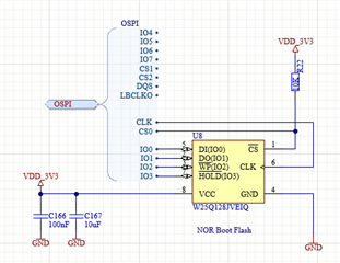
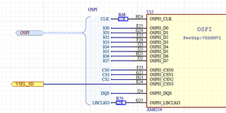
We are facing problem when connecting a SPI Nor (W25Q128VEIQ) to OSPI CS0.

Basically it is working but from time to time it comes to errors during SF PROBE command in u.boot.

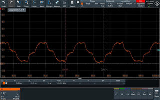
Please find attached the CLK Signal measured during sf probe.

Do you have any advice why the CLK Singal has this strange shape?

The CLK is running at 83.3Mhz
Many thanks and best regards

Stephan

  • Hello Stephan, 

    Thank you for the inputs.

    Can you please provide additional input on the setup including inputs about the board if this a custom board?

    Regards,

    Sreenivasa

  • Hello Sreenivasa
    We made a custom Module with the AM6254.
    The SPI Nor is connected to OSPI CS0

    Here is the devicetree of uboot for the spinor config:

    &ospi0 {
        pinctrl-names = "default";
        pinctrl-0 = <&ospi0_pins_default>;
        status = "okay";

        flash@0{
            compatible = "jedec,spi-nor";
            reg = <0x0>;
            spi-tx-bus-width = <4>;
            spi-rx-bus-width = <4>;
            spi-max-frequency = <133000000>;

            partitions {
                compatible = "fixed-partitions";
                #address-cells = <1>;
                #size-cells = <1>;

                partition@0 {
                    label = "ospi.tiboot3";
                    reg = <0x0 0x80000>;
                };

                partition@80000 {
                    label = "ospi.tispl";
                    reg = <0x80000 0x200000>;
                };

                partition@280000 {
                    label = "ospi.u-boot";
                    reg = <0x280000 0x400000>;
                };

                partition@680000 {
                    label = "ospi.env";
                    reg = <0x680000 0x40000>;
                };

                partition@6c0000 {
                    label = "ospi.env.backup";
                    reg = <0x6c0000 0x40000>;
                };

                partition@800000 {
                    label = "ospi.rootfs";
                    reg = <0x800000 0x800000>;
                };
            };
        };

    Do you have any hint how to configure ospi correctly for standard qspi interface?

    Many thanks and best regards

    Stephan

  • Hello Stephan

    Thank you for the inputs.

    Since it works most of the time, I will help check if there are any issues with the hardware. 

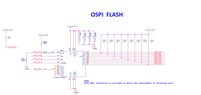
    Do you have provision for termination similar to the below EVM diagram?

    Can you help understand the clock length 

    Regards,

    Sreenivasa

  • Hello Sreenivasa

    I have a 22R Series Termination close to the CPU PAD H24. I don't have the 100k Pulldown on the CLK like R311 on the EVM.

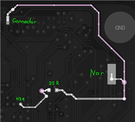
    The CLK is routed from the PCU PAD H24 to 22R series termination to the SPI Nor and then to a connector Pad for future use of another OSPI or simmilar device.
     

    The trace from CPU Pad H24 to 22R is 3.6mm

    The trace from 22R to SPI Nor PAD6 is 8mm,
    then from SPI Nor PAD6 to the Module Connector 14.4mm
    The complete CLK Track lenght is 26mm.

    Here is an illustration of the CLK Track

    For the measurement i posted above, the Connector pad is floating and not connected to any device.

    Best regards

    Stephan

  • Hello Stephan

    Thank you for the inputs.

    Can you please help me understand the probing point for the waveform.

    What is the clock speed that you are running. Did you try increasing the series resistor.

    Are the clock and data pins length matched.

    Regards,

    Sreenivasa

  • Hello Sreenivasa

    The clockspeed is 83.3Mhz

    I probed the CLK on the Pad of the SPI Nor with reference to GND very close.
    The Tracks are not lenght matched but they are routed 50 Ohm single ended.

  • I personally think it is a mistake providing multiple chip select pins on this peripheral. It is misleading and makes someone think they can connect multiple devices, when this implementation is very problematic. 

    The problem with connecting multiple devices is related to your observation on the clock. You see this distortion on the source end of the signal trace because the output buffer has about the same source impedance as the signal trace. When the signal changes from low to high or high to low, the voltage applied to the signal is divided by the ratio of output buffer source impedance and the signal trace impedance. It is basically a voltage divider that results in a mid-supply voltage being applied to the signal. This mid-supply voltage propagates down the signal trace until it encounters a high-impedance or open-circuit, where the mismatch in impedance results in an in-phase reflection that causes the voltage at the far end to make a continuous transition from VDD to VSS or VSS to VDD. This reflection returns back to the source, where the voltage at the source will not continue to VDD or VSS until this reflection has returned. The length of the mid-supply step function will be equal to two times the propagation time of the clock signal trace. The step function gets shorter as you get closer to the end of the signal trace, but not completely gone until the very end.

    A device connected anywhere other than the far end of the signal trace will observe the same step function on the clock signal. Connecting a device clock input anywhere in the middle of a clock signal trace is a very bad design practice because there is a good chance the output of the clock input buffer of this device will generate internal clock glitches when this mid-supply voltage pauses near the switching threshold of the input buffer. You cannot split the signal trace into two paths without creating impedance discontinuities which also causes signal distortion. Inserting buffers will resolve the impedance mismatch issue but inserts delay in the clock path, which may cause a timing violation because the peripheral was timing closed assuming a direct connection without any buffer delays.

    Connecting your NOR memory device to the middle of the clock signal was a mistake. You must resolve this issue by disconnecting any signal trace that extends beyond the attached device to prevent any internal clock glitch issues.

    Most of the AM62x pins power-up turned off, so you need include external pull resistors to hold any attached device inputs in a valid logic state until the IOs and associated peripheral module has been initialized by software. You should never allow CMOS inputs to float. this is especially true for the AM62x inputs. All AM62x inputs which have been enabled must be held in a valid logic state that is above the VIHSS or VILSS as defined in the respective electrical characteristics section of the datasheet. The AM62x device could be damaged if your design allows any enabled inputs to float to mid-supply voltages for an accumulated period of time over the life of the product.

    Regards,
    Paul