Part Number: AM3356
Hi,
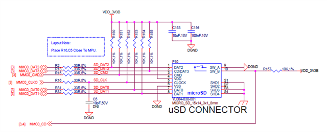
Planning to use the MMC0 interface of AM3356 for SD Card interface to the processor.
Checked the datasheet and there was no detail on the Layout and Routing recommendations for SD Interface.
Planning to use the below Pins from Processor to connect a uSD interface.
What all are the points to be taken care of on the Design stage and please share the recommended layout guidelines to match the processor requirements.
Also, Please suggest if anything is to be done carefully while doing the design/Layout.
The current allocation from Processor perspective is given below:
|
Pin |
MMC Signals |
|
G15 |
MMC0_DAT1 |
|
F18 |
MMC0_DAT2 |
|
F17 |
MMC0_DAT3 |
|
G16 |
MMC0_DAT0 |
|
G17 |
MMC0_CLK |
|
G18 |
MMC0_CMD |
|
A13 |
MMC0_SDCD |
---
Thanks & Regards,
Akshay V