Hello Champs,
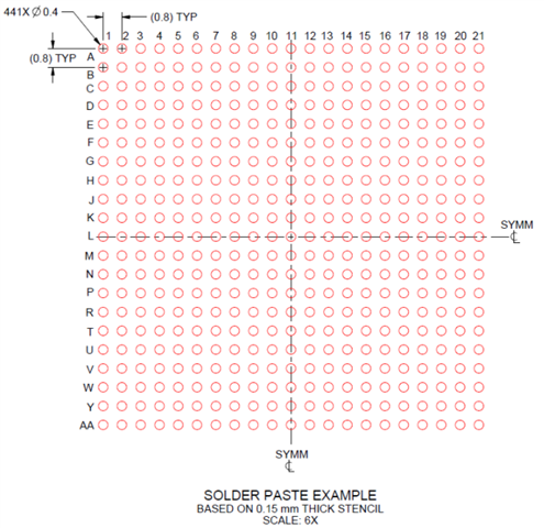
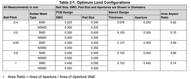
It requires 0.15mm thick stencil in datasheet spec. But many pcb manufacturers usually use 0.1mm or 0.12mm thick stencil. Can customer change the thick stencil to 0.1mm? Will it cause some soldering issues?


Thanks
Rgds
Shine
This thread has been locked.
If you have a related question, please click the "Ask a related question" button in the top right corner. The newly created question will be automatically linked to this question.
Hello Champs,
It requires 0.15mm thick stencil in datasheet spec. But many pcb manufacturers usually use 0.1mm or 0.12mm thick stencil. Can customer change the thick stencil to 0.1mm? Will it cause some soldering issues?


Thanks
Rgds
Shine
Hello Shine
Thank you for the note.
The amount of the paste is dependent on the stencil thickness.
The .127 thickness would be a possibility if customer can make some changes to ensure that the solder paste to solder the ball is available.
I will check internally and update you on the feasibility.
Regards,
Sreenivasa
Hi Sreenivasa
So there's no way to go below .10mm ~.12mm thickness?
R0402 / R0201 / C0402 / C0201 is the mainstream material, the steel plate is recommended to be .12mm~.10mm, and hope that TI will introduce a version below .12mm.
BR,
Taylor
Hello Taylor,
Currently it looks to be so.
Let me check internally.
I do not have a timeline.
Do you want to close the thread and ping back later sometime next year?
Regards,
Sreenivasa
Hello Taylor,
We have a number of app noted that can be referenced. The PCB pad size, PCB solder mask opening size, and stencil thickness guidelines provided by TI are meant to be a good starting point.
There are many variables that come into play which may require these parameters to be adjusted. For example, some PCBs may warp during reflow worse than other PCBs, which requires more solder paste volume to be deposited to achieve reliable connectivity. The solder paste volume required to achieve good connective can also vary from one type of solder paste to another type of solder paste. The thickness of the stencil and shape of the apertures may need to be adjusted to deposit an appropriate volume of solder paste on the PCB. The PCB assembly vendor may need to perform many trial runs adjusting these parameters until they develop a reliable recipe the specific combination of PCB and components being installed on the PCB.
Below is one of the app note link and the required info captured.
https://www.ti.com/lit/an/spraa99c/spraa99c.pdf

Regards,
Sreenivasa
Hello Taylor,
Here are the additional inputs i received
When we design the PCB land pad and stencil, we will look at the substrate pad size, solder ball dimension and ball pitch to come up the optimized design to obtain a good solder joint.
This will be validated by running BLR (Board level reliability) to look at the joint reliability.
Reducing the stencil thickness will reduce the total solder paste volume affecting the final joint shape and standoff. Increasing
the stencil aperture to compensate the volume may not work since the paste pattern will be different so as the final joint shape.
If a customer want to reduce the stencil thickness because of other Components on their board, then I would suggest them to consider
using a step up stencil (different stencil thickness at different location).
Regards,
Sreenivasa
Hi Sreenivasa
Thanks for your suggestion.
Different stencil thicknesses in different positions will be included in the control of other projects in the follow-up. It is not the best way, but thank you for your reply.
BR,
Taylor
Hello Taylor,
Thank you for the inputs and appreciate your thoughts.
I will close the thread if you do not have additional queries.
Regards,
Sreenivasa