This thread has been locked.

If you have a related question, please click the "Ask a related question" button in the top right corner. The newly created question will be automatically linked to this question.

AM625: OSPI timing question

Part Number: AM625
Other Parts Discussed in Thread: AM6442

Hi,

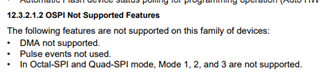
The AM625 Datasheet diagram for OSPI Tap mode SDR shows sampling on falling edge (Figure 7-102). We are operating in SPI Mode 0 (drive on SCLK falling edge, sample on SCLK rising edge). Does this edge change depending on SPI mode?


RD_DATA_CAPTURE_REG has a SAMPLE_EDGE_SEL_FLD bit, could we get a description on what this register does? “SAMPLE_EDGE_SEL_FLD bit selects the edge of the reference clock, on which data outputs from flash memory are sampled", but the datasheet diagram shows it sampling on an SCLK edge, not an RCLK edge. Is there a picture that can explain this?

Thank You

  • Greetings Brad,

    Gentle FYI, the AM62 TRM is not posted but you can use AM6442 as reference, SPI modes other than 0 in Octal or Quad mode are not supported. To answer your question, the IP follows the same modes as the SPI standard with clock polarity and phase changing across modes.

    The SCLK (source clock output to the flash) is sourced directly from the RCLK (reference clock inside the SoC), though depending on the mode this can be divided down by the baud rate divider inside the IP(Tap Mode) or output 1:1 (PHY mode). In either case they are phase aligned, you can consider changing the SAMPLE_EDGE_SEL_FLD as changing which edge of the SCLK the IP will sample data from the flash from. 

    Sincerely,

    Lucas

  • Lucas,

    Thanks for your response. Customer has some follow-up.

    I think we’ll need some follow-up since that didn’t quite answer what we’re looking for, or maybe we just need some clarifications.


    Basically we’re trying to figure out exactly when the sampling occurs (i.e. what point the setup and hold times are relative to).  Figure 7-102 is our reference, but I think it is incomplete and/or misleading.  There are a few register settings that seem like they should change that sampling point, but it isn’t clear how all of these register settings relate to this Figure.


    On our first question:  We’re operating in mode 0, so the part about other modes not being supported doesn’t apply to us.  The problem is that there’s a discrepancy between the mode 0 description (sample on SCLK rising edge) vs. Figure 7-102 (which pictures it sampling on the SCLK falling edge).  Our thought is that Figure 7-102 might be showing mode 1 or mode 2 operation where sampling would occur on the SCLK falling edge.


    • Can you confirm that when it is set to use mode 0, the setup and hold times should be measured relative to the SCLK rising edge (not the falling edge as shown in Figure 7-102)?
    • Or if I’m interpreting the E2E response correctly, RD_DATA_CAPTURE_REG[5] SAMPLE_EDGE_SEL_FLD determines the SCLK edge that it samples on, despite the separate registers that select the mode, and despite the TRM description (in Section 12.4.2.4.2.1.2) that this register chooses the RCLK (not SCLK) edge.  Is this the correct interpretation?  What is the polarity of this register?  We’ll want to set it to sample on the SCLK rising edge.


    On our second question:  Our understanding is that the sampling actually occurs on an RCLK edge, T RCLK cycles after an SCLK edge (where T is selected by RD_DATA_CAPTURE_REG[4:1] DELAY_FLD, and our first question is meant to figure out which SCLK edge that we start counting from).  We are using TAP mode and dividing RCLK to get SCLK.


    • If that second bullet above is not the right interpretation, I do not know how to interpret SAMPLE_EDGE_SEL_FLD, but my guess is that it would move the sample point by an extra ½ RCLK cycle to sample on the selected RCLK edge.  If that is correct, we would need to know the polarity relationship between RCLK and SCLK (does SCLK toggle on an RCLK rising or falling edge?) and the polarity of this SAMPLE_EDGE_SEL_FLD register (does a value of 1 mean it samples on RCLK’s rising or falling edge?).  This is where a timing diagram would be helpful.


    Thanks!

  • Greetings Brad,

    Parameters O19 and O20 are relative to whichever edge of the OSPI_CLK is active, in this case it'd be the rising edge since data is being sampled from the flash on that edge. The figure is only a reference one to show the relationship between the edge of a clock (in that case a falling edge) to data for setup and hold, but again the parameters are for whichever edge is active.

    First question: I think I understand what's being asked a little better now, how about this for an explanation:

    In Tap SDR mode, you can likely achieve a valid sampling configuration with either using the falling or rising edge of the reference clock; since it runs at 4x (or rather the SCLK is divided down by 4x from the ref clk), there are possibly multiple sampling configurations that can be achieved based off other delays in the system. My initial answer was simplified and best practice, as if you were to switch strategies to using PHY mode later on it would need to be aligned with what the edge the memory outputs on (PHY mode outputs 1:1 reference clock to SCLK). Considering this: 

    • If it is set to mode 0 where the active edge for sampling data is the rising edge, the setup and hold times are relative to the rising edge.
    • RD_DATA_CAPTURE_REG[5] SAMPLE_EDGE_SEL_FLD determines the reference clock edge the IP uses to sample data. In other modes besides Tap SDR this clock can be 1:1 to other modes (so the clocks can be considered the same), I'd recommend keeping it to the same edge. In Tap SDR mode you will likely be able to achieve valid configurations with either edge. The TRM also has descriptions for this register, using the AM64x TRM as reference it is 12.3.2.6.11 OSPI_RD_DATA_CAPTURE_REG Register.

    Second question: I don't quite see a direct question, but I will try to address the concern I'm interpreting:

    • Sampling occurs internally from the reference clock, but the setup and hold times in the datasheet are relative to the active edge of the SCLK (which can be either technically, in Mode 0 it is the rising edge). The TRM has a description of the RD_DATA_CAPTURE_REG[5] SAMPLE_EDGE_SEL_FLD, for the AM64x TRM (which can be used as reference for AM62) in 12.3.2.6.11 OSPI_RD_DATA_CAPTURE_REG Register.
    • The reference clock and SCLK are in phase with the same polarity, as SCLK is a divided down reference clock. 

    In actuality there are likely sub-sets of valid configurations you could achieve for any given combination of flash device (with each device having different delay times for output) and board topology (which affects the propagation of the data from the flash to the SoC relative to the clock being output from the SoC). The first portion of the OSPI datasheet has the PCB connectivity requirements for OSPI signals.

    RD_DATA_CAPTURE_REG[4:1] DELAY_FLD is chiefly used to compensate for this delay, as sampling can be delayed by reference clock cycles to mimic the delay the flash and/or board topology can cause. Even if you try to calculate "the value" to use for this register, in some cases a range of values can work. If this is a concern for large productions we'd recommend in characterization of your boards/setup to try and find the range of values to use for your unique topology and flash choice; if there is more than value one pick the middle of them for your final SW configuration. Faux training every time can also be implemented to find the most robust value for this field as well.

    A similar case for RD_DATA_CAPTURE_REG[5] SAMPLE_EDGE_SEL_FLD, you can vary the sampling edge if actually needed, but we recommend keeping it in line with the edge the flash outputs data. Again, in some modes the reference clock is output 1:1 to the SCLK and changing this setting could result in functional failure. For Tap SDR mode, you may find changing this field does nothing; the way the IP does sampling in tap mode( if the reference clock is 4x the SCLK) then sampling will occur correctly in the majority of setups with either edge.

    The biggest factors to setup and hold time are detailed in the datasheet, which is the minimum setup and hold time shifted by the RD_DATA_CAPTURE_REG[4:1] DELAY_FLD settings. This is again relative to the active SCLK edge which for Mode 0 is the rising edge.

    I hope my response helped, for the second question I attempted to address the question behind the question regarding concern over finding the optimal register values. 

    Sincerely,

    Lucas

  • Greetings Brad,

    If there are no other questions, I am closing this thread. Please follow up as necessary.