I am using 3 SPI cores in my project. We are facing the following issues
- SPI1 and SPI2 are working properly
- Data in serial terminal is as expected
- Probed data also as expected
- Both are working in 10MHz
- SPI3 is having the following issues
- Data on MISO is displaying as 'FF; in serial terminal
- MISO pins are probed and expected data is observed
- The slave device is taking the command so that MOSI is working as expected
- MISO pins also probed and Observed as expected
- Clocks and CSn is probed and observed as expected
- We reduced the clock frequency to 1.5MHz, but same observations
- I compared clock signal of SPI1 and SPI3 and both are same (No noise/ disturbance observed)
Below mentioned are the pinmux configurations that am using while configuring MCSPI
| MCSPI | Chip Select | Ball Pins | Address | Value |
| MCSPI 1 | CS 0 | B24 | 0x4A0037B0 | 0x00020000 |
| CS 1 | C25 | 0x4A0037B4 | 0x00020000 | |
| Clk | C24 | 0x4A0037A4 | 0x00050000 | |
| MOSI | D25 | 0x4A0037AC | 0x00050000 | |
| MISO | D24 | 0x4A0037A8 | 0x00050000 | |
| Clk Enable | - | 0x4A0097F0 | 0x00000002 | |
| MCSPI 2 | CS 0 | F24 | 0x4A0037CC | 0x00020000 |
| CS 2 | E24 | 0x4A0037B8 | 0x00020003 | |
| Clk | G25 | 0x4A0037C0 | 0x00050000 | |
| MOSI | G24 | 0x4A0037C8 | 0x00050000 | |
| MISO | F25 | 0x4A0037C4 | 0x00050000 | |
| Clk Enable | - | 0x4A0097F8 | 0x00000002 | |
| MCSPI 3 | CS 0 | B18 | 0x4A0036E0 | 0x00020003 |
| CS 1 | A19 | 0x4A0036E4 | 0x00020003 | |
| Clk | A18 | 0x4A0036D4 | 0x00050003 | |
| MOSI | B16 | 0x4A0036DC | 0x00050003 | |
| MISO | B17 | 0x4A0036D8 | 0x00050003 | |
| Clk Enable | - | 0x4A009800 | 0x00000002 |
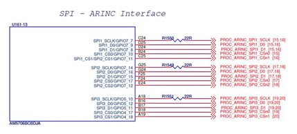
Below mentioned is the schemantic of the MCSPI

Please help me solve this issue
Regards,
Sarath

