This thread has been locked.

If you have a related question, please click the "Ask a related question" button in the top right corner. The newly created question will be automatically linked to this question.

TDA2HG: internal structure of RSTOUTN (F23 PIN)

Part Number: TDA2HG

Hi team,

Here's an issue from the customer may need your help:

The RSTOUTN (F23 PIN) pin is still measured to be 3.3 V with both a pullup (3.3 V) and a pulldown applied externally.

So the customer would like to know what is the internal circuitry for this pin? When internally configured as a pull-up, does it not affect the level even if a pull-down resistor is added externally? And what structure does the internal pull-up look like? PMOS strong pull-up?

The following is the customer's schematic:

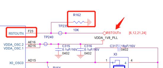
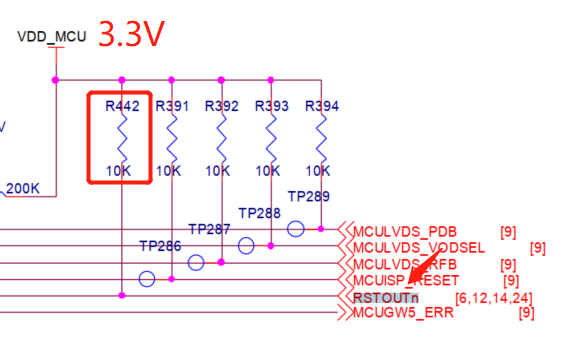
Could you help check this case? Thanks.

Best Regards,

Cherry

  • RSTOUTn is a driven output (not open drain).  As stated in the processor data manual, RSTOUTn is only valid after VDDSHV3 is valid.  If the RSTOUTn signal is to be used as a reset into other devices, it must be AND'd with PORz to prevent glitches during power ramping periods.  The pull-down is placed to help keep the signal low during power ramping - but again recommend AND'd with PORz input.

  • Hi Robert,

    Thanks for your support. May I know if it's proper to disclose the response on public forum?

    RSTOUTn is a driven output (not open drain). 

    What's the difference of "driven output" and "open drain"? Is driven output refer to push-pull circuit? And is the output of the push-pull circuit unaffected when pulled up or down? 

    Thanks and regards,

    Cherry

  • Yes - output is push-pull circuit.  Yes - pull-down is only affective during periods of when the device is powering-up or powering down.