A related question is a question created from another question. When the related question is created, it will be automatically linked to the original question.
If you have a related question, please click the "Ask a related question" button in the top right corner. The newly created question will be automatically linked to this question.
DM3730: Schematic & layout guidance document of DM3730
For our now-used CPU platform, there is not much guidance for the GPMC bus. Are there any other documents about GPMC BUS usage, I believe another platform is ok, just need more info here.
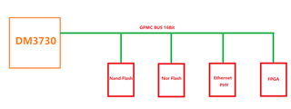
Below is the topology of our current design, for now, they want to know the GPMC BUS stub line length / the total length limit, the Parasitic capacitance requirements, which is critical for our design, the maximum number of peripheral devices that are supported.
The datasheet shows that the timings apply with typical capacitive loading of 12pF - See Table 6-2. GPMC/NOR Flash Timing Conditions—Synchronous Mode https://www.ti.com/lit/gpn/dm3730
For trace lengths, need to perform timing analysis. Perhaps the IBIS model could be used to simulate with the 4 loads and stubs. A 3D extraction of the board would provide best results. Clock buffering may be required like a 1 to 4 buffer.
Is this design using synchronous or asynch mode? How fast or slow does the system operate?